AMD
P R E L I M I N A R Y
to delay the start of CRC8 and CRC32 and DC bias control
calculation for both receive and transmit frames. The physical
header field is assumed to begin after the Start of Frame Delimiter
has been detected.
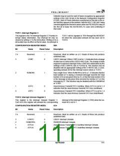
TCR4: Antenna Diversity Timer
This register is the Antenna Diversity Timer register
used to control antenna dwell time during antenna
diversity measurements.
CONFIGURATION REGISTER INDEX:
04h
Bit
Name
Reset Value
Description
7
ANTEN
0
Antenna Diversity Enable. When set to a 1, the internal antenna di-
versity logic is used to select the antenna. When set to a 0, software
has control over antenna selection through the ANTS bit of
TIR26[4] and the ANTSLTLD bit of TCR7[1]. Dwell times for an-
tenna measurements are still used to obtain RSSI data when this bit
is set to 0, but final antenna selection will be controlled by software.
6
Reserved
ADT[5:0]
–
Reserved. Must be written as a 0. Reads of this bit produce
undefined data.
5–0
00h
Antenna Diversity Timer. Dwell time per antenna in time steps of
CLKIN period times 20 when the CLKGT20 bit of MIR9 is set to 0,
and time steps of CLKIN period times 40, when the CLKGT20 bit of
MIR9 is set to 1. When the value in this register is “00,” then the di-
versity switching function is disabled.
TCR5: TX Ramp Up Timing
This register is the TX Ramp Up Timing register. This
register determines the ramp up timing of the TX
enable signals.
CONFIGURATION REGISTER INDEX:
05h
Bit
Name
Reset Value
Description
7:4
TGAP1[3:0]
0h
Transmit Timing Gap 1. These bits are used to determine the gap
between the assertion of the T1 signal and the assertion of the T2
signal. T1 and T2 can be used to control the timing of the TXCMD
and TXPE pins, respectively. The interval is programmable with a
resolution equal to 20 times the CLKIN period when the CLKGT20
bit of MIR9 is set to 0 and a resolution equal to 40 times the CLKIN
period when the CLKGT20 bit of MIR9 is set to 1. For a 1Mbs data
rate with CLKIN = 20MHz and CLKGT20 = 0, the resolution is 1 µ.
3:0
TGAP2[3:0]
0h
Transmit Timing Gap 2. These bits are used to determine the gap
between the assertion of the T2 signal and the assertion of the T3
signal. The interval is programmable with a resolution equal to 20
times the CLKIN period when the CLKGT20 bit of MIR9 is set to 0
and a resolution equal to 40 times the CLKIN period when the
CLKGT20 bit of MIR9 is set to 1. For a 1 Mbs data rate with CLKIN =
20 MHz and CLKGT20 = 0, the resolution is 1 µ.
Am79C930
107

 AMD [ AMD ]