D A T A S H E E T
TABLE OF CONTENTS
Product Selector Guide. . . . . . . . . . . . . . . . . . . . . 4
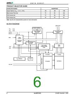
Block Diagram . . . . . . . . . . . . . . . . . . . . . . . . . . . . 4
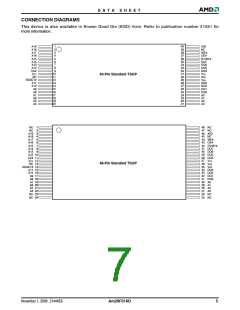
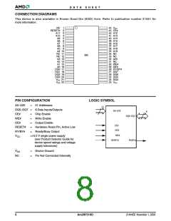
Connection Diagrams . . . . . . . . . . . . . . . . . . . . . . 5
Pin Configuration. . . . . . . . . . . . . . . . . . . . . . . . . . 6
Logic Symbol . . . . . . . . . . . . . . . . . . . . . . . . . . . . . 6
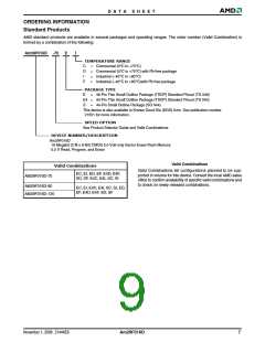
Ordering Information. . . . . . . . . . . . . . . . . . . . . . . 7
Device Bus Operations . . . . . . . . . . . . . . . . . . . . . 8
Table 1. Am29F016D Device Bus Operations .................................. 8
Requirements for Reading Array Data ..................................... 8
Writing Commands/Command Sequences .............................. 8
Program and Erase Operation Status ...................................... 9
Standby Mode .......................................................................... 9
RESET#: Hardware Reset Pin ................................................. 9
Output Disable Mode................................................................ 9
Table 2. Sector Address Table........................................................ 10
Autoselect Mode..................................................................... 11
Table 3. Am29F016D Autoselect Codes (High Voltage Method).... 11
Sector Group Protection/Unprotection.................................... 11
Table 4. Sector Group Addresses................................................... 11
Temporary Sector Group Unprotect ....................................... 11
Figure 1. Temporary Sector Group Unprotect Operation............... 12
Hardware Data Protection ...................................................... 12
Low VCC Write Inhibit...................................................................... 12
Write Pulse “Glitch” Protection........................................................ 12
Logical Inhibit .................................................................................. 12
Power-Up Write Inhibit .................................................................... 12
Common Flash Memory Interface (CFI) . . . . . . . 13
Table 5. CFI Query Identification String.......................................... 13
Table 6. System Interface String..................................................... 13
Table 7. Device Geometry Definition .............................................. 14
Table 8. Primary Vendor-Specific Extended Query ........................ 14
Command Definitions . . . . . . . . . . . . . . . . . . . . . 15
Reading Array Data................................................................ 15
Reset Command..................................................................... 15
Autoselect Command Sequence............................................ 15
Byte Program Command Sequence....................................... 15
Unlock Bypass Command Sequence.............................................. 16
Figure 2. Program Operation ......................................................... 16
Chip Erase Command Sequence........................................... 16
Sector Erase Command Sequence........................................ 17
Erase Suspend/Erase Resume Commands........................... 17
Figure 3. Erase Operation.............................................................. 18
Command Definitions ............................................................. 19
Table 9. Am29F016D Command Definitions................................... 19
Write Operation Status . . . . . . . . . . . . . . . . . . . . 20
DQ7: Data# Polling................................................................. 20
Figure 4. Data# Polling Algorithm ................................................. 20
RY/BY#: Ready/Busy#............................................................ 21
DQ6: Toggle Bit I.................................................................... 21
DQ2: Toggle Bit II................................................................... 21
Reading Toggle Bits DQ6/DQ2............................................... 21
DQ5: Exceeded Timing Limits ................................................ 22
DQ3: Sector Erase Timer ....................................................... 22
Figure 5. Toggle Bit Algorithm....................................................... 22
Table 10. Write Operation Status................................................... 23
Absolute Maximum Ratings. . . . . . . . . . . . . . . . . 24
Figure 6. Maximum Negative Overshoot Waveform ..................... 24
Figure 7. Maximum Positive Overshoot Waveform....................... 24
Operating Ranges. . . . . . . . . . . . . . . . . . . . . . . . . 24
DC Characteristics . . . . . . . . . . . . . . . . . . . . . . . . 25
TTL/NMOS Compatible .......................................................... 25
CMOS Compatible.................................................................. 25
Test Conditions. . . . . . . . . . . . . . . . . . . . . . . . . . . 26
Figure 8. Test Setup..................................................................... 26
Table 11. Test Specifications......................................................... 26
Key to Switching Waveforms. . . . . . . . . . . . . . . . 26
AC Characteristics . . . . . . . . . . . . . . . . . . . . . . . . 27
Read-only Operations............................................................. 27
Figure 9. Read Operation Timings................................................ 27
Figure 10. RESET# Timings ......................................................... 28
Erase/Program Operations..................................................... 29
Figure 11. Program Operation Timings......................................... 30
Figure 12. Chip/Sector Erase Operation Timings ......................... 31
Figure 13. Data# Polling Timings (During Embedded Algorithms) 32
Figure 14. Toggle Bit Timings (During Embedded Algorithms)..... 32
Figure 15. DQ2 vs. DQ6................................................................ 33
Figure 16. Temporary Sector Group Unprotect Timings............... 33
Erase and Program Operations.............................................. 34
Alternate CE# Controlled Writes .................................................... 34
Figure 17. Alternate CE# Controlled Write Operation Timings ..... 35
Erase and Programming Performance . . . . . . . 36
Latchup Characteristics. . . . . . . . . . . . . . . . . . . . 36
TSOP and SO Pin Capacitance . . . . . . . . . . . . . . 36
Data Retention. . . . . . . . . . . . . . . . . . . . . . . . . . . . 36
Physical Dimensions . . . . . . . . . . . . . . . . . . . . . . 37
TS 040—40-Pin Standard Thin Small Outline Package ......... 37
TS 048—48-Pin Standard Thin Small Outline Package ......... 38
SO 044—44-Pin Small Outline Package ................................ 39
Revision Summary . . . . . . . . . . . . . . . . . . . . . . . . 40
November 2, 2006 21444E6
Am29F016D
3

 AMD [ AMD ]