D A T A S H E E T
GENERAL DESCRIPTION
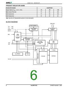
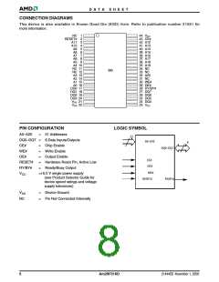
The Am29F016D is a 16 Mbit, 5.0 volt-only Flash mem-
ory organized as 2,097,152 bytes. The 8 bits of data
appear on DQ0–DQ7. The Am29F016D is offered in
48-pin TSOP, 40-pin TSOP, and 44-pin SO packages.
The device is also available in Known Good Die (KGD)
form. For more information, refer to publication number
21551. This device is designed to be programmed
algorithm—an internal algorithm that automatically
preprograms the array (if it is not already programmed)
before executing the erase operation. During erase, the
device automatically times the erase pulse widths and
verifies proper cell margin.
The host system can detect whether a program or
erase operation is complete by observing the RY/BY#
pin, or by reading the DQ7 (Data# Polling) and DQ6
(toggle) status bits. After a program or erase cycle has
been completed, the device is ready to read array data
or accept another command.
in-system with the standard system 5.0 volt V supply.
CC
A 12.0 volt V is not required for program or erase
PP
operations. The device can also be programmed in
standard EPROM programmers.
This device is manufactured using AMD’s 0.23 µm pro-
cess technology, and offers all the features and
benefits of the Am29F016, which was manufactured
using 0.5 µm process technology.
The sector erase architecture allows memory sectors
to be erased and reprogrammed without affecting the
data contents of other sectors. The device is fully
erased when shipped from the factory.
The standard device offers access times of 70, 90, and
120 ns, allowing high-speed microprocessors to oper-
ate without wait states. To eliminate bus contention, the
device has separate chip enable (CE#), write enable
(WE#), and output enable (OE#) controls.
Hardware data protection measures include a low
V
detector that automatically inhibits write opera-
CC
tions during power transitions. The hardware sector
protection feature disables both program and erase
operations in any combination of the sectors of mem-
ory. This can be achieved via programming equipment.
The device requires only a single 5.0 volt power sup-
ply for both read and write functions. Internally
generated and regulated voltages are provided for the
program and erase operations.
The Erase Suspend feature enables the user to put
erase on hold for any period of time to read data from,
or program data to, any sector that is not selected for
erasure. True background erase can thus be achieved.
The device is entirely command set compatible with the
JEDEC single-power-supply Flash standard. Com-
mands are written to the command register using
standard microprocessor write timings. Register con-
tents serve as input to an internal state-machine that
controls the erase and programming circuitry. Write cy-
cles also internally latch addresses and data needed
for the programming and erase operations. Reading
data out of the device is similar to reading from other
Flash or EPROM devices.
The hardware RESET# pin terminates any operation
in progress and resets the internal state machine to
reading array data. The RESET# pin may be tied to the
system reset circuitry. A system reset would thus also
reset the device, enabling the system microprocessor
to read the boot-up firmware from the Flash memory.
The system can place the device into the standby
mode. Power consumption is greatly reduced in
this mode.
Device programming occurs by executing the program
command sequence. This initiates the Embedded
Program algorithm—an internal algorithm that auto-
matically times the program pulse widths and verifies
proper cell margin.
AMD’s Flash technology combines years of Flash
memory manufacturing experience to produce the
highest levels of quality, reliability and cost effective-
ness. The device electrically erases all bits within a
sector simultaneously via Fowler-Nordheim tunneling.
The data is programmed using hot electron injection.
Device erasure occurs by executing the erase com-
mand sequence. This initiates the Embedded Erase
2
Am29F016D
21444E6 November 1, 2006

 AMD [ AMD ]