P R E L I M I N A R Y
sectors of memory), the system must drive WE# and
within the same bank (except the sector being erased).
Figure 19 shows how read and write cycles may be in-
itiated for simultaneous operation with zero latency.
ICC6 and ICC7 in the DC Characteristics table represent
the current specifications for read-while-program and
read-while-erase, respectively.
CE# to VIL, and OE# to VIH.
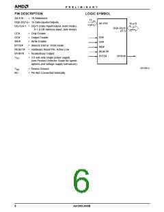
For program operations, the BYTE# pin determines whether
the device accepts program data in bytes or words. Refer to
“Word/Byte Configuration” for more information.
The device features an Unlock Bypass mode to facili-
tate faster programming. Once a bank enters the Unlock
Bypass mode, only two write cycles are required to pro-
gram a word or byte, instead of four. The “Byte/Word
Program Command Sequence” section has details on
programming data to the device using both standard and
Unlock Bypass command sequences.
Standby Mode
When the system is not reading or writing to the device,
it can place the device in the standby mode. In this
mode, current consumption is greatly reduced, and the
outputs are placed in the high impedance state, inde-
pendent of the OE# input.
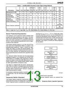
An erase operation can erase one sector, multiple sec-
tors, or the entire device. Tables 2 and 3 indicate the
address space that each sector occupies. The device
address space is divided into two banks: Bank 1 con-
tains the boot/parameter sectors, and Bank 2 contains
the larger, code sectors of uniform size. A “bank ad-
dress” is the address bits required to uniquely select a
bank. Similarly, a “sector address” is the address bits
required to uniquely select a sector.
The device enters the CMOS standby mode when the
CE# and RESET# pins are both held at VCC ± 0.3 V.
(Note that this is a more restricted voltage range than
VIH.) If CE# and RESET# are held at VIH, but not within
V
CC ± 0.3 V, the device will be in the standby mode, but
the standby current will be greater. The device requires
standard access time (tCE) for read access when the
device is in either of these standby modes, before it is
ready to read data.
If the system writes the autoselect command se-
quence, the device enters the autoselect mode. The
system can then read autoselect codes from the inter-
nal register (which is separate from the memory array)
on DQ7–DQ0. Standard read cycle timings apply in this
mode. Refer to the Autoselect Mode and Autoselect
Command Sequence sections for more information.
If the device is deselected during erasure or program-
ming, the device draws active current until the
operation is completed.
ICC3 in the DC Characteristics table represents the
standby current specification.
Automatic Sleep Mode
ICC2 in the DC Characteristics table represents the ac-
tive current specification for the write mode. The AC
Characteristics section contains timing specification ta-
bles and timing diagrams for write operations.
The automatic sleep mode minimizes Flash device
energy consumption. The device automatically enables
this mode when addresses remain stable for tACC + 30
ns. The automatic sleep mode is independent of the
CE#, WE#, and OE# control signals. Standard address
access timings provide new data when addresses are
changed. While in sleep mode, output data is latched
and always available to the system. ICC4 in the DC
Characteristics table represents the automatic sleep
mode current specification.
Simultaneous Read/Write Operations with
Zero Latency
This device is capable of reading data from one bank of
memory while programming or erasing in the other
bank of memory. An erase operation may also be sus-
pended to read from or program to another location
Am29DL800B
9

 AMD [ AMD ]