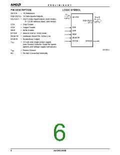
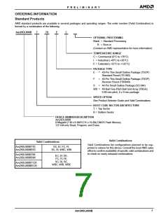
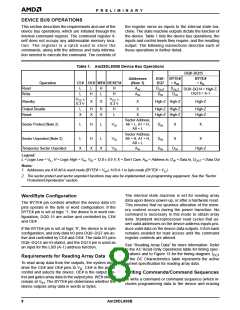
P R E L I M I N A R Y
memory, enabling the system to read the boot-up
RESET#: Hardware Reset Pin
firmware from the Flash memory.
The RESET# pin provides a hardware method of reset-
ting the device to reading array data. When the RE-
SET# pin is driven low for at least a period of tRP, the
device immediately terminates any operation in
progress, tristates all output pins, and ignores all read/
write commands for the duration of the RESET# pulse.
The device also resets the internal state machine to
reading array data. The operation that was interrupted
should be reinitiated once the device is ready to accept
another command sequence, to ensure data integrity.
If RESET# is asserted during a program or erase oper-
ation, the RY/BY# pin remains a “0” (busy) until the in-
ternal reset operation is complete, which requires a
time of tREADY (during Embedded Algorithms). The
system can thus monitor RY/BY# to determine whether
the reset operation is complete. If RESET# is asserted
when a program or erase operation is not executing
(RY/BY# pin is “1”), the reset operation is completed
within a time of tREADY (not during Embedded Algo-
rithms). The system can read data tRH after the RE-
SET# pin returns to VIH.
Current is reduced for the duration of the RESET#
pulse. When RESET# is held at VSS±0.3 V, the device
draws CMOS standby current (ICC4). If RESET# is held
at VIL but not within VSS±0.3 V, the standby current will
be greater.
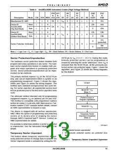
Refer to the AC Characteristics tables for RESET# pa-
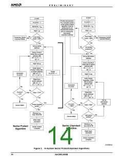
rameters and to Figure 14 for the timing diagram.
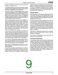
Output Disable Mode
The RESET# pin may be tied to the system reset cir-
cuitry. A system reset would thus also reset the Flash
When the OE# input is at VIH, output from the device is
disabled. The output pins are placed in the high imped-
ance state.
10
Am29DL800B

 AMD [ AMD ]