P R E L I M I N A R Y
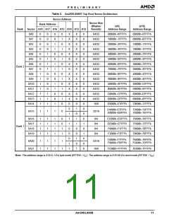
DEVICE BUS OPERATIONS
This section describes the requirements and use of the
device bus operations, which are initiated through the
internal command register. The command register it-
self does not occupy any addressable memory loca-
tion. The register is a latch used to store the
commands, along with the address and data informa-
tion needed to execute the command. The contents of
the register serve as inputs to the internal state ma-
chine. The state machine outputs dictate the function of
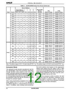
the device. Table 1 lists the device bus operations, the
inputs and control levels they require, and the resulting
output. The following subsections describe each of
these operations in further detail.
Table 1. Am29DL800B Device Bus Operations
DQ8–DQ15
BYTE#
= V
Addresses
(Note 1)
DQ0– BYTE#
Operation
CE# OE# WE# RESET#
DQ7
= V
IH
IL
Read
L
L
H
H
A
D
D
DQ8–DQ14 = High-Z,
DQ15 = A-1
IN
OUT
OUT
Write
L
H
L
H
A
D
D
IN
IN
IN
V
0.3 V
±
V
0.3 V
±
CC
CC
Standby
X
X
X
High-Z High-Z
High-Z
Output Disable
Reset
L
H
X
H
X
H
L
X
X
High-Z High-Z
High-Z High-Z
High-Z
High-Z
X
Sector Address,
A6 = L, A1 = H,
A0 = L
Sector Protect (Note 2)
L
H
L
V
D
X
X
X
ID
IN
Sector Address,
A6 = H, A1 = H,
A0 = L
Sector Unprotect (Note 2)
L
H
X
L
V
V
D
D
X
ID
ID
IN
IN
Temporary Sector Unprotect
X
X
A
D
High-Z
IN
IN
Legend:
L = Logic Low = V , H = Logic High = V , V = 12.0 ± 0.5 V, X = Don’t Care, A = Address In, D = Data In, D = Data Out
IL
IH
ID
IN
IN
OUT
Notes:
1. Addresses are A18:A0 in word mode (BYTE# = V ), A18:A-1 in byte mode (BYTE# = V ).
IH
IL
2. The sector protect and sector unprotect functions may also be implemented via programming equipment. See the “Sector
Protection/Unprotection” section.
The internal state machine is set for reading array
Word/Byte Configuration
data upon device power-up, or after a hardware reset.
The BYTE# pin controls whether the device data I/O
This ensures that no spurious alteration of the mem-
pins operate in the byte or word configuration. If the
ory content occurs during the power transition. No
BYTE# pin is set at logic ‘1’, the device is in word con-
command is necessary in this mode to obtain array
figuration, DQ0-15 are active and controlled by CE#
data. Standard microprocessor read cycles that as-
and OE# .
sert valid addresses on the device address inputs pro-
If the BYTE# pin is set at logic ‘0’, the device is in byte
configuration, and only data I/O pins DQ0–DQ7 are ac-
tive and controlled by CE# and OE#. The data I/O pins
DQ8–DQ14 are tri-stated, and the DQ15 pin is used as
an input for the LSB (A-1) address function.
duce valid data on the device data outputs. EAch bank
remains enabled for read access until the command
register contents are altered.
See “Reading Array Data” for more information. Refer
to the AC Read-Only Operations table for timing spec-
ifications and to Figure 13 for the timing diagram. ICC1
in the DC Characteristics table represents the active
current specification for reading array data.
Requirements for Reading Array Data
To read array data from the outputs, the system must
drive the CE# and OE# pins to VIL. CE# is the power
control and selects the device. OE# is the output con-
trol and gates array data to the output pins. WE# should
remain at VIH. The BYTE# pin determines whether the
device outputs array data in words or bytes.
Writing Commands/Command Sequences
To write a command or command sequence (which in-
cludes programming data to the device and erasing
8
Am29DL800B

 AMD [ AMD ]