P R E L I M I N A R Y
DQ6 also toggles during the erase-suspend-program
RY/BY#: Ready/Busy#
mode, and stops toggling once the Embedded Pro-
gram algorithm is complete.
The RY/BY# is a dedicated, open-drain output pin that
indicates whether an Embedded Algorithm is in
progress or complete. The RY/BY# status is valid after
the rising edge of the final WE# pulse in the command
sequence. Since RY/BY# is an open-drain output, sev-
eral RY/BY# pins can be tied together in parallel with a
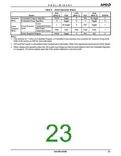
Table 6 shows the outputs for Toggle Bit I on DQ6. Fig-
ure 6 shows the toggle bit algorithm. Figure 21 in the
“AC Characteristics” section shows the toggle bit timing
diagrams. Figure 22 shows the differences between
DQ2 and DQ6 in graphical form. See also the subsec-
tion on DQ2: Toggle Bit II.
pull-up resistor to VCC
.
If the output is low (Busy), the device is actively erasing
or programming. (This includes programming in the
Erase Suspend mode.) If the output is high (Ready),
the device is ready to read array data, is in the standby
mode, or one of the banks is in the erase-suspend-read
mode.
DQ2: Toggle Bit II
The “Toggle Bit II” on DQ2, when used with DQ6, indi-
cates whether a particular sector is actively erasing
(that is, the Embedded Erase algorithm is in progress),
or whether that sector is erase-suspended. Toggle Bit
II is valid after the rising edge of the final WE# pulse in
the command sequence.
Table 6 shows the outputs for RY/BY#.
DQ6: Toggle Bit I
DQ2 toggles when the system reads at addresses
within those sectors that have been selected for eras-
ure. (The system may use either OE# or CE# to control
the read cycles.) But DQ2 cannot distinguish whether
the sector is actively erasing or is erase-suspended.
DQ6, by comparison, indicates whether the device is
actively erasing, or is in Erase Suspend, but cannot dis-
tinguish which sectors are selected for erasure. Thus,
both status bits are required for sector and mode infor-
mation. Refer to Table 6 to compare outputs for DQ2
and DQ6.
Toggle Bit I on DQ6 indicates whether an Embedded
Program or Erase algorithm is in progress or complete,
or whether the device has entered the Erase Suspend
mode. Toggle Bit I may be read at any address within
the programming or erasing bank, and is valid after the
rising edge of the final WE# pulse in the command se-
quence (prior to the program or erase operation), and
during the sector erase time-out.
During an Embedded Program or Erase algorithm op-
eration, successive read cycles to any address within
the programming or erasing bank cause DQ6 to toggle.
The system may use either OE# or CE# to control the
read cycles. When the operation is complete, DQ6
stops toggling.
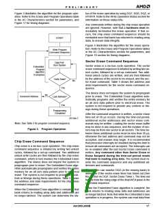
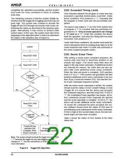
Figure 6 shows the toggle bit algorithm in flowchart
form, and the section “DQ2: Toggle Bit II” explains the
algorithm. See also the DQ6: Toggle Bit I subsection.
Figure 21 shows the toggle bit timing diagram. Figure
22 shows the differences between DQ2 and DQ6 in
graphical form.
After an erase command sequence is written, if all sec-
tors selected for erasing are protected, DQ6 toggles for
approximately 100 µs, then returns to reading array
data. If not all selected sectors are protected, the Em-
bedded Erase algorithm erases the unprotected sec-
tors, and ignores the selected sectors that are
protected.
Reading Toggle Bits DQ6/DQ2
Refer to Figure 6 for the following discussion. Whenever
the system initially begins reading toggle bit status, it
must read DQ7–DQ0 at least twice in a row to determine
whether a toggle bit is toggling. Typically, the system
would note and store the value of the toggle bit after the
first read. After the second read, the system would com-
pare the new value of the toggle bit with the first. If the
toggle bit is not toggling, the device has completed the
program or erase operation. The system can read array
data on DQ7–DQ0 on the following read cycle.
The system can use DQ6 and DQ2 together to deter-
mine whether a sector is actively erasing or is erase-
suspended. When a bank is actively erasing (that is,
the Embedded Erase algorithm is in progress), DQ6
toggles. When that bank enters the Erase Suspend
mode, DQ6 stops toggling. However, the system must
also use DQ2 to determine which sectors are erasing
or erase-suspended. Alternatively, the system can use
DQ7 (see the subsection on DQ7: Data# Polling).
However, if after the initial two read cycles, the system
determines that the toggle bit is still toggling, the sys-
tem also should note whether the value of DQ5 is high
(see the section on DQ5). If it is, the system should
then determine again whether the toggle bit is toggling,
since the toggle bit may have stopped toggling just as
DQ5 went high. If the toggle bit is no longer toggling,
the device has successfully completed the program or
erase operation. If it is still toggling, the device did not
If a program address falls within a protected sector,
DQ6 toggles for approximately 1 µs after the program
command sequence is written, then returns to reading
array data.
Am29DL800B
21

 AMD [ AMD ]