P R E L I M I N A R Y
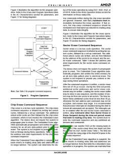
Figure 3 illustrates the algorithm for the program oper-
tus of the erase operation by using DQ7, DQ6, DQ2, or
RY/BY#. Refer to the Write Operation Status section for
information on these status bits.
ation. Refer to the Erase and Program Operations table
in the AC Characteristics section for parameters, and
Figure 17 for timing diagrams.
Any commands written during the chip erase operation
are ignored. However, note that a hardware reset im-
mediately terminates the erase operation. If that oc-
curs, the chip erase command sequence should be
reinitiated once that bank has returned to reading array
data, to ensure data integrity.
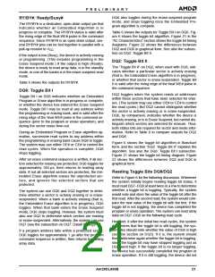
START
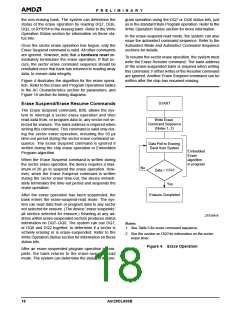
Figure 4 illustrates the algorithm for the erase opera-
tion. Refer to the Erase and Program Operations tables
in the AC Characteristics section for parameters, and
Figure 18 section for timing diagrams.
Write Program
Command Sequence
Sector Erase Command Sequence
Data Poll
from System
Sector erase is a six bus cycle operation. The sector
erase command sequence is initiated by writing two un-
lock cycles, followed by a set-up command. Two addi-
tional unlock cycles are written, and are then followed
by the address of the sector to be erased, and the sec-
tor erase command. Table 5 shows the address and
data requirements for the sector erase command se-
quence.
Embedded
Program
algorithm
in progress
Verify Data?
No
Yes
The device does not require the system to preprogram
prior to erase. The Embedded Erase algorithm auto-
matically programs and verifies the entire memory for
an all zero data pattern prior to electrical erase. The
system is not required to provide any controls or tim-
ings during these operations.
No
Increment Address
Last Address?
Yes
Programming
Completed
After the command sequence is written, a sector erase
time-out of 50 µs occurs. During the time-out period,
additional sector addresses and sector erase com-
mands may be written. Loading the sector erase buffer
may be done in any sequence, and the number of sec-
tors may be from one sector to all sectors. The time be-
tween these additional cycles must be less than 50 µs,
otherwise the last address and command may not be
accepted, and erasure may begin. It is recommended
that processor interrupts be disabled during this time to
ensure all commands are accepted. The interrupts can
be re-enabled after the last Sector Erase command is
written. Any command other than Sector Erase or
Erase Suspend during the time-out period resets
that bank to reading array data. The system must re-
write the command sequence and any additional ad-
dresses and commands.
21519A-7
Note: See Table 5 for program command sequence.
Figure 3. Program Operation
Chip Erase Command Sequence
Chip erase is a six bus cycle operation. The chip erase
command sequence is initiated by writing two unlock
cycles, followed by a set-up command. Two additional
unlock write cycles are then followed by the chip erase
command, which in turn invokes the Embedded Erase
algorithm. The device does not require the system to
preprogram prior to erase. The Embedded Erase algo-
rithm automatically preprograms and verifies the entire
memory for an all zero data pattern prior to electrical
erase. The system is not required to provide any con-
trols or timings during these operations. Table 5 shows
the address and data requirements for the chip erase
command sequence.
The system can monitor DQ3 (in the erasing bank) to
determine if the sector erase timer has timed out (See
the section on DQ3: Sector Erase Timer.). The time-out
begins from the rising edge of the final WE# pulse in the
command sequence.
When the Embedded Erase algorithm is complete, the
bank returns to reading array data and addresses are
no longer latched. Note that while the Embedded Erase
operation is in progress, the system can read data from
When the Embedded Erase algorithm is complete, that
bank returns to reading array data and addresses are
no longer latched. The system can determine the sta-
Am29DL800B
17

 AMD [ AMD ]