P R E L I M I N A R Y
completed the operation successfully, and the system
must write the reset command to return to reading
array data.
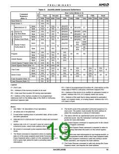
DQ5: Exceeded Timing Limits
DQ5 indicates whether the program or erase time has
exceeded a specified internal pulse count limit. Under
these conditions DQ5 produces a “1,” indicating that
the program or erase cycle was not successfully com-
pleted.
The remaining scenario is that the system initially de-
termines that the toggle bit is toggling and DQ5 has not
gone high. The system may continue to monitor the
toggle bit and DQ5 through successive read cycles, de-
termining the status as described in the previous para-
graph. Alternatively, it may choose to perform other
system tasks. In this case, the system must start at the
beginning of the algorithm when it returns to determine
the status of the operation (top of Figure 6).
The device may output a “1” on DQ5 if the system tries
to program a “1” to a location that was previously pro-
grammed to “0.” Only an erase operation can change
a “0” back to a “1.” Under this condition, the device
halts the operation, and when the timing limit has been
exceeded, DQ5 produces a “1”.
Under both these conditions, the system must write the
reset command to return to reading array data (or to the
erase-suspend-read mode if a bank was previously in
the erase-suspend-program mode).
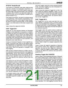
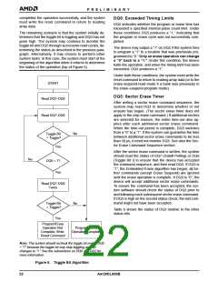
START
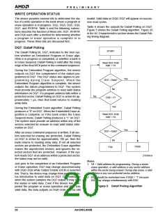
DQ3: Sector Erase Timer
Read DQ7–DQ0
After writing a sector erase command sequence, the
system may read DQ3 to determine whether or not
erasure has begun. (The sector erase timer does not
apply to the chip erase command.) If additional sectors
are selected for erasure, the entire time-out also ap-
plies after each additional sector erase command.
When the time-out period is complete, DQ3 switches
from a “0” to a “1”. If the system can guarantee the time
between additional sector erase commands to be less
than 50 µs, it need not monitor DQ3. See also the Sec-
tor Erase Command Sequence section.
Read DQ7–DQ0
No
Toggle Bit
= Toggle?
Yes
After the sector erase command is written, the system
should read the status of DQ7 (Data# Polling) or DQ6
(Toggle Bit I) to ensure that the device has accepted
the command sequence, and then read DQ3. If DQ3 is
“1”, the Embedded Erase algorithm has begun; all fur-
ther commands (except Erase Suspend) are ignored
until the erase operation is complete. If DQ3 is “0”, the
device will accept additional sector erase commands.
To ensure the command has been accepted, the sys-
tem software should check the status of DQ3 prior to
and following each subsequent sector erase command.
If DQ3 is high on the second status check, the last com-
mand might not have been accepted.
No
DQ5 = 1?
Yes
Read DQ7–DQ0
Twice
Toggle Bit
= Toggle?
No
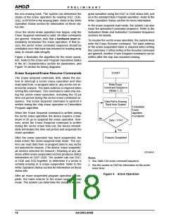
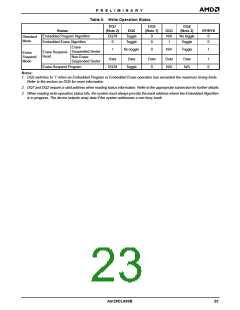
Table 6 shows the status of DQ3 relative to the other
status bits.
Yes
Program/Erase
Operation Not
Complete, Write
Reset Command
Program/Erase
Operation Complete
Note: The system should recheck the toggle bit even if DQ5
= “1” because the toggle bit may stop toggling as DQ5
changes to “1.” See the subsections on DQ6 and DQ2 for
more information.
Figure 6. Toggle Bit Algorithm
22
Am29DL800B

 AMD [ AMD ]