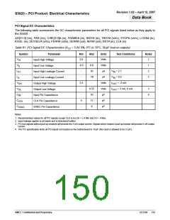
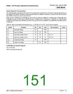
Revision 1.02 – April 12, 2007
S5920 – PCI Product: Electrical Characteristics
Data Book
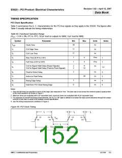
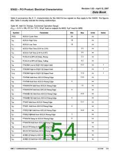
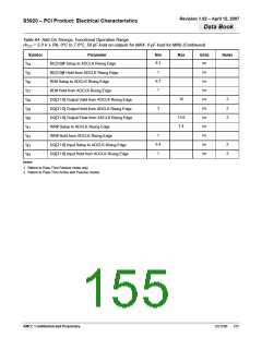
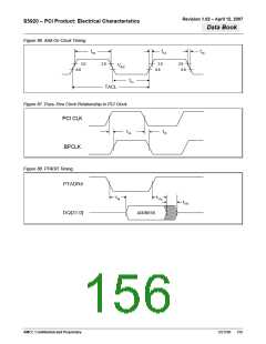
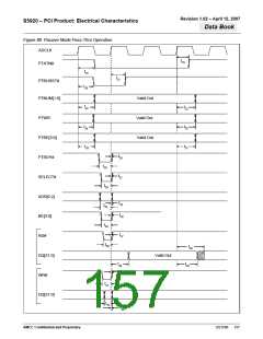
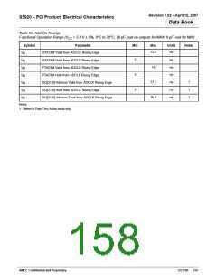
Table 6 summarizes the A. C. characteristics for the Add-On bus signals as they apply to the S5920. The figures
after Table 6 visually indicate the timing relationships.
Table 64. Add-On Timings, Functional Operation Range
(V = 5.0 V ± 5%, 0°C to 7 0°C, 50 pF load on outputs for MAX, 0 pF load for MIN)
CC
Symbol
TACL
Parameter
Min
25
Max
Units
ns
Notes
ADCLK Cycle Time
ADCLK High Time
ADCLK Low Time
t
t
t
t
t
t
t
t
t
t
t
t
t
t
t
t
t
t
t
t
t
t
t
t
t
10
ns
10
11
10
ns
ns
ns
ns
ns
ns
ns
ns
ns
ns
ns
ns
ns
ns
ns
ns
ns
ns
ns
ns
ns
ns
ns
ns
2.5
2.5
ADCLK Rise Time (0.8V to 2.0V)
12
13
14
15
16
17a
17b
18
19
20
21
22
23
24
25
26
27
28
29
30
31
32
33
ADCLK Fall Time (2.0V to 0.8V)
5.3
PCICLK to BPCLK Delay, Rising
6.2
PCICLK to BPCLK Delay, Falling
13.1
1
1
1
PTADR# Low to DQ[31:0] Output Valid
PTADR# High to DQ[31:0] Output Hold
PTADR# High to DQ[31:0] Output Float
PTATN# Valid from ADCLK Rising Edge
PTATN# Hold from ADCLK Rising Edge
PTBURST# Valid from ADCLK Rising Edge
PTBURST# Hold from ADCLK Rising Edge
PTNUM[1:0] Valid from ADCLK Rising Edge
PTNUM[1:0] Hold from ADCLK Rising Edge
PTWR Valid from ADCLK Rising Edge
PTWR Hold from ADCLK Rising Edge
PTBE[3:0]# Valid from ADCLK Rising Edge
PTBE[3:0]#Hold from ADCLK Rising Edge
PTWAIT# Setup to ADCLK Rising Edge
PTWAIT# Hold from ADCLK Rising Edge
SELECT# Setup to ADCLK Rising Edge
SELECT# Hold from ADCLK Rising Edge
ADR[6:2] Setup to ADCLK Rising Edge
ADR[6:2] Hold from ADCLK Rising Edge
2
11.9
13.5
4
4
4
4
13
14.4
13.1
14.4
3
11
1
8.9
1
9.3
1
AMCC Confidential and Proprietary
DS1596
154

 AMCC [ APPLIED MICRO CIRCUITS CORPORATION ]