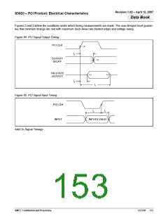
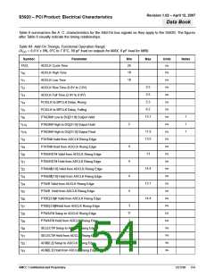
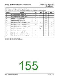
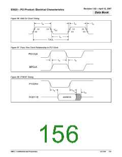
PDF
最近搜索
热门搜索
发布采购

| 型号: | S5920QRC |
| PDF下载: | 下载PDF文件 查看货源 |
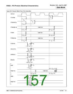
| 内容描述: | [PCI Bus Controller, CMOS, PQFP160, 28 X 28 MM, 3.37 MM HEIGHT, GREEN, PLASTIC, QFP-160] |
| 分类和应用: | 时钟数据传输PC外围集成电路 |
| 文件页数/大小: | 165 页 / 2405 K |
| 品牌: |  AMCC [ APPLIED MICRO CIRCUITS CORPORATION ] AMCC [ APPLIED MICRO CIRCUITS CORPORATION ] |
专业IC领域供求交易平台:提供全面的IC Datasheet资料和资讯,Datasheet 1000万数据,IC品牌1000多家。