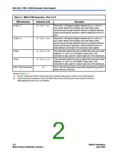
In System Programmability
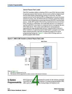
General-Purpose Flash Loader
The JTAG translator ability to interface JTAG to non-JTAG devices is ideal
for general-purpose flash memory devices (such as Intel or Fujitsu based
devices) that require programming during in-circuit test. The flash
memory devices can be used for FPGA configuration or be part of system
memory. In many cases, the MAX II device is already connected to these
devices as the configuration control logic between the FPGA and the flash
device. Unlike ISP-capable CPLD devices, bulk flash devices do not have
JTAG TAP pins or connections. For small flash devices, it is common to
use the serial JTAG scan chain of a connected device to program the non-
JTAG flash device. This is slow and inefficient in most cases and
impractical for large parallel flash devices. Using the MAX II device’s
JTAG translator as a general-purpose flash loader to program and verify
flash contents provides a fast and cost-effective means of in-circuit
programming during test. Figure 3–1 shows MAX II being used as a
general-purpose flash loader.
Figure 3–1. MAX II JTAG Translator as General-Purpose Flash Loader
MAX II Device
Flash
Memory Device
DQ[7..0]
DQ[7..0]
A[20..0]
OE
A[20..0]
OE
WE
WE
CE
CE
RY/BY
RY/BY
TDO_U
TDI_U
General-
Purpose
Flash Loader
Logic
TDI
TMS
TCK
TMS_U
TCK_U
SHIFT_U
CLKDR_U
(1),(2)
TDO
UPDATE_U
RUNIDLE_U
USER1_U
Notes to Figure 3–1:
(1) This block is implemented in LEs.
(2) This function will be supported in a future version of the Quartus II software.
MAX II devices can be programmed in-system via the industry standard
4-pin IEEE Std. 1149.1 (JTAG) interface. In system programmability (ISP)
offers quick, efficient iterations during design development and
In System
Programmability
3–4
Core Version a.b.c variable
Altera Corporation
June 2004
MAX II Device Handbook, Volume 1

 ALTERA [ ALTERA CORPORATION ]