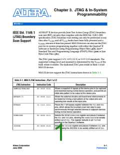
JTAG & In-System Programmability
The MAX II device instruction register length is 10 bits and the USERCODE
register length is 32 bits. Tables 3–2 and 3–3 show the boundary-scan
register length and device IDCODEinformation for MAX II devices.
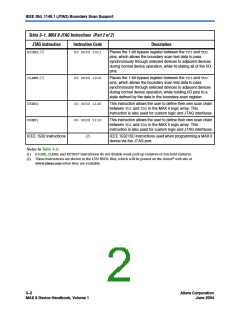
Table 3–2. MAX II Boundary-Scan Register Length
Device
Boundary-Scan Register Length
EPM240
EPM570
240
480
636
816
EPM1270
EPM2210
Table 3–3. 32-Bit MAX II Device IDCODE
Binary IDCODE (32 Bits) (1)
Device
HEX IDCODE
Version
(4 Bits)
Manufacturer
Identity (11 Bits)
LSB
(1 Bit) (2)
Part Number
EPM240
EPM570
EPM1270
EPM2210
0000
0000
0000
0000
0010 0000 1010 0001
0010 0000 1010 0010
0010 0000 1010 0011
0010 0000 1010 0100
000 0110 1110
000 0110 1110
000 0110 1110
000 0110 1110
1
1
1
1
0x020A10DD
0x020A20DD
0x020A30DD
0x020A40DD
Notes to Table 3–2:
(1) The most significant bit (MSB) is on the left.
(2) The IDCODE's least significant bit (LSB) is always 1.
f
For JTAG AC characteristics, refer to the chapter on DC & Switching
Characteristics. For more information on JTAG BST, see the chapter on
IEEE 1149.1 (JTAG) Boundary-Scan Testing for MAX II Devices.
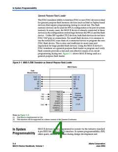
JTAG Translator
The JTAG translator feature allows you to access the JTAG TAP and state
signals when either the USER0or USER1instruction is issued to the JTAG
TAP. The USER0and USER1instructions bring the JTAG boundary scan
chain (TDI) through the user logic instead of the MAX II device’s
boundary scan cells. Each USERinstruction allows for one unique user-
defined JTAG chain into the logic array.
Altera Corporation
June 2004
Core Version a.b.c variable
3–3
MAX II Device Handbook, Volume 1

 ALTERA [ ALTERA CORPORATION ]