IEEE Std. 1149.1 (JTAG) Boundary Scan Support
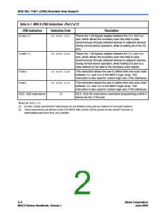
Table 3–1. MAX II JTAG Instructions (Part 2 of 2)
JTAG Instruction
Instruction Code
Description
HIGHZ(1)
00 0000 1011
Places the 1-bit bypass register between the TDIand TDO
pins, which allows the boundary scan test data to pass
synchronously through selected devices to adjacent devices
during normal device operation, while tri-stating all of the I/O
pins.
CLAMP(1)
00 0000 1010
Places the 1-bit bypass register between the TDIand TDO
pins, which allows the boundary scan test data to pass
synchronously through selected devices to adjacent devices
during normal device operation, while holding I/O pins to a
state defined by the data in the boundary-scan register.
USER0
USER1
00 0000 1100
00 0000 1110
(2)
This instruction allows the user to define their own scan chain
between TDIand TDOin the MAX II logic array. This
instruction is also used for custom logic and JTAG interfaces.
This instruction allows the user to define their own scan chain
between TDIand TDOin the MAX II logic array. This
instruction is also used for custom logic and JTAG interfaces.
IEEE 1532 instructions
IEEE 1532 ISC instructions used when programming a MAX II
device via the JTAG port.
Notes to Table 3–1:
(1) HIGHZ, CLAMP, and EXTESTinstructions do not disable weak pull-up resistors or bus hold features.
(2) These instructions are shown in the 1532 BSDL files, which will be posted on the Altera® web site at
www.altera.com when they are available.
3–2
Core Version a.b.c variable
Altera Corporation
June 2004
MAX II Device Handbook, Volume 1

 ALTERA [ ALTERA CORPORATION ]