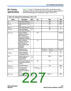
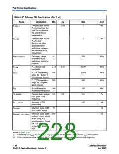
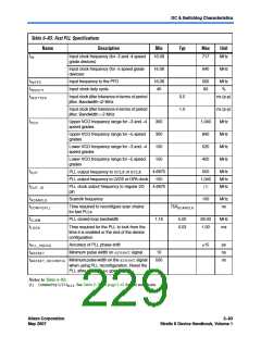
DC & Switching Characteristics
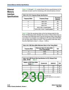
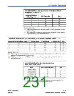
Table 5–97. DQS Phase Jitter Specifications for DLL-Delayed Clock
(tDQS PHASE_JITTER) Note (1)
Number of DQS Delay
Buffer Stages (2)
DQS Phase Jitter
Unit
1
2
3
4
30
60
ps
ps
ps
ps
90
120
Notes to Table 5–97:
(1) Peak-to-peak phase jitter on the phase shifted DDS clock (digital jitter is caused
by DLL tracking).
(2) Delay stages used for requested DQS phase shift are reported in your project’s
Compilation Report in the Quartus II software.
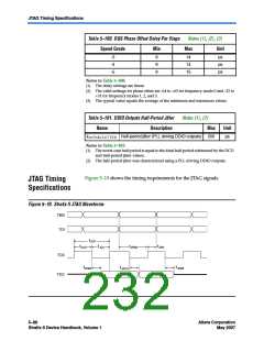
Table 5–98. DQS Phase-Shift Error Specifications for DLL-Delayed Clock (tDQS_PSERR)
(1)
Number of DQS Delay Buffer Stages (2) –3 Speed Grade –4 Speed Grade –5 Speed Grade
Unit
1
2
3
4
25
50
30
60
35
70
ps
ps
ps
ps
75
90
105
140
100
120
Note to Table 5–98:
(1) This error specification is the absolute maximum and minimum error. For example, skew on three delay buffer
stages in a C3 speed grade is 75 ps or 37.5 ps.
(2) Delay stages used for requested DQS phase shift are reported in your project’s Compilation Report in the
Quartus II software.
Table 5–99. DQS Bus Clock Skew Adder Specifications
(tDQS_CLOCK_SKEW_ADDER)
Mode
DQS Clock Skew Adder
Unit
×4 DQ per DQS
×9 DQ per DQS
×18 DQ per DQS
×36 DQ per DQS
40
70
75
95
ps
ps
ps
ps
Note to Table 5–99:
(1) This skew specification is the absolute maximum and minimum skew. For
example, skew on a ×4 DQ group is 40 ps or 20 ps.
Altera Corporation
May 2007
5–95
Stratix II Device Handbook, Volume 1

 ALTERA [ ALTERA CORPORATION ]