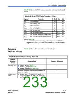
Document Revision History
Table 5–103. Document Revision History (Part 2 of 3)
Date and
Document
Version
Changes Made
Summary of Changes
April 2006, v4.1
●
●
●
●
Updated Table 5–3.
Updated Table 5–11.
Updated Figures 5–8 and 5–9.
●
●
●
Changed 0.2 MHz to 2 MHz in
Table 5–93.
Added new spec for half period
jitter (Table 5–101).
Added support for PLL clock
switchover for industrial
temperature range.
Changed fINPFD (min) spec from
4 MHz to 2 MHz in Table 5–92.
Fixed typo in tOUTJITTER
specification in Table 5–92.
Updated VDIF AC & DC max
specifications in Table 5–28.
Updated minimum values for tJCH
tJCL, and tJPSU in Table 5–102.
Update maximum values for tJPCO
tJPZX, and tJPXZ in Table 5–102.
Added parallel on-chip termination information to
“On-Chip Termination Specifications” section.
Updated Tables 5–28, 5–30,5–31, and 5–34.
Updated Table 5–78, Tables 5–81 through 5–90,
and Tables 5–92, 5–93, and 5–98.
Updated “PLL Timing Specifications” section.
Updated “External Memory Interface
Specifications” section.
●
●
●
●
●
●
●
●
●
●
●
Added Tables 5–95 and 5–101.
Updated “JTAG Timing Specifications” section,
including Figure 5–10 and Table 5–102.
,
,
December 2005,
v4.0
●
Updated “External Memory Interface
Specifications” section.
—
●
●
Updated timing numbers throughout chapter.
July 2005, v3.1
Updated HyperTransport technology information in
Table 5–13.
—
●
●
●
Updated “Timing Model” section.
Updated “PLL Timing Specifications” section.
Updated “External Memory Interface
Specifications” section.
May 2005, v3.0
●
●
●
●
Updated tables throughout chapter.
Updated “Power Consumption” section.
Added various tables.
Replaced “Maximum Input & Output Clock Rate”
section with “Maximum Input & Output Clock Toggle
Rate” section.
—
●
●
Added “Duty Cycle Distortion” section.
Added “External Memory Interface Specifications”
section.
March 2005,
v2.2
Updated tables in “Internal Timing Parameters”
section.
—
—
January 2005,
v2.1
Updated input rise and fall time.
5–98
Altera Corporation
May 2007
Stratix II Device Handbook, Volume 1

 ALTERA [ ALTERA CORPORATION ]