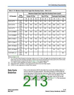
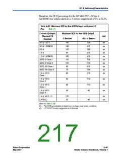
Duty Cycle Distortion
Figure 5–7. Duty Cycle Distortion
Ideal Falling Edge
CLKH = T/2
CLKL = T/2
D1
D2
Falling Edge A
Falling Edge B
Clock Period (T)
DCD expressed in absolution derivation, for example, D1 or D2 in
Figure 5–7, is clock-period independent. DCD can also be expressed as a
percentage, and the percentage number is clock-period dependent. DCD
as a percentage is defined as
(T/2 – D1) / T (the low percentage boundary)
(T/2 + D2) / T (the high percentage boundary)
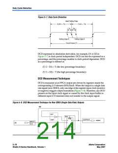
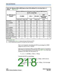
DCD Measurement Techniques
DCD is measured at an FPGA output pin driven by registers inside the
corresponding I/O element (IOE) block. When the output is a single data
rate signal (non-DDIO), only one edge of the register input clock (positive
or negative) triggers output transitions (Figure 5–8). Therefore, any DCD
present on the input clock signal or caused by the clock input buffer or
different input I/O standard does not transfer to the output signal.
Figure 5–8. DCD Measurement Technique for Non-DDIO (Single-Data Rate) Outputs
IOE
NOT
DFF
PRN
OUTPUT
inst1
output
D
Q
INPUT
VCC
clk
CLRN
inst
5–78
Altera Corporation
May 2007
Stratix II Device Handbook, Volume 1

 ALTERA [ ALTERA CORPORATION ]