DC & Switching Characteristics
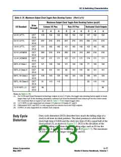
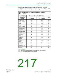
Table 5–79. Maximum Output Clock Toggle Rate Derating Factors (Part 5 of 5)
Maximum Output Clock Toggle Rate Derating Factors (ps/pF)
Drive
Strength
I/O Standard
Column I/O Pins
Row I/O Pins
Dedicated Clock Outputs
-3
-4
-5
-3
-4
-5
-3
-4
-5
3.3-V LVTTL
OCT
50 Ω
133
207
151
300
157
121
56
152
152
133
152
152
147
152
152
2.5-V LVTTL
OCT
50 Ω
274
165
316
171
134
101
123
110
-
274
165
316
171
134
101
123
110
-
207
151
300
157
121
56
274
165
316
171
134
101
123
-
274
165
316
171
134
101
123
-
235
153
263
174
77
274
165
316
171
134
101
123
110
-
274
165
316
171
134
101
123
110
95
1.8-V LVTTL
OCT
50 Ω
3.3-V LVCMOS
1.5-V LVCMOS
SSTL-2 Class I
SSTL-2 Class II
SSTL-18 Class I
SSTL-18 Class II
1.2-V HSTL (2)
OCT
50 Ω
OCT
50 Ω
OCT
50 Ω
OCT
25 Ω
58
OCT
50 Ω
100
61
100
-
106
59
OCT
25 Ω
OCT
95
-
-
-
-
50 Ω
Notes to Table 5–79:
(1) For LVDS and HyperTransport technology output on row I/O pins, the toggle rate derating factors apply to loads
larger than 5 pF. In the derating calculation, subtract 5 pF from the intended load value in pF for the correct result.
For a load less than or equal to 5 pF, refer to Table 5–78 for output toggle rates.
(2) 1.2-V HSTL is only supported on column I/O pins in I/O banks 4,7, and 8.
(3) Differential HSTL and SSTL is only supported on column clock and DQS outputs.
(4) LVPECL is only supported on column clock outputs.
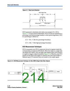
Duty cycle distortion (DCD) describes how much the falling edge of a
clock is off from its ideal position. The ideal position is when both the
clock high time (CLKH) and the clock low time (CLKL) equal half of the
clock period (T), as shown in Figure 5–7. DCD is the deviation of the
non-ideal falling edge from the ideal falling edge, such as D1 for the
falling edge A and D2 for the falling edge B (Figure 5–7). The maximum
DCD for a clock is the larger value of D1 and D2.
Duty Cycle
Distortion
Altera Corporation
May 2007
5–77
Stratix II Device Handbook, Volume 1

 ALTERA [ ALTERA CORPORATION ]