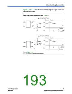
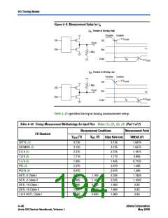
DC and Switching Characteristics
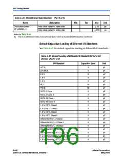
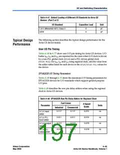
Table 4–47. Default Loading of Different I/O Standards for Arria GX
Devices (Part 2 of 2)
I/O Standard
Capacitive Load
Unit
1.8-V differential HSTL Class II
LVDS
0
0
pF
pF
The following section describes the typical design performance for the
Arria GX device family.
Typical Design
Performance
User I/O Pin Timing
Tables 4–48 to 4–77 show user I/O pin timing for Arria GX devices. I/O
buffer tSU, tH, and tCO are reported for the cases when I/O clock is driven
by a non-PLL global clock (GCLK) and a PLL driven global clock
(GCLK-PLL). For tSU, tH, and tCO using regional clock, add the value from
the adder tables listed for each device to the GCLK/GCLK-PLLvalues for
the device.
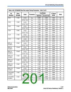
EP1AGX20 I/O Timing Parameters
Tables 4–48 through 4–51 show the maximum I/O timing parameters for
EP1AGX20 devices for I/O standards which support general purpose
I/O pins.
Table 4–48 describes the row pin delay adders when using the regional
clock in Arria GX devices.
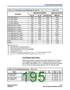
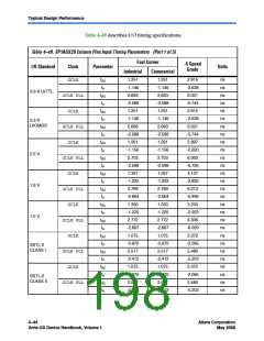
Table 4–48. EP1AGX20 Row Pin Delay Adders for Regional Clock
Fast Corner
-6 Speed
Parameter
Units
ns
Grade
Industrial
Commercial
0.117
0.117
0.273
RCLKinput
adder
0.011
-0.117
-0.011
0.011
-0.117
-0.011
0.019
-0.273
-0.019
ns
RCLKPLL
input adder
ns
RCLK output
adder
ns
RCLKPLL
output adder
Altera Corporation
May 2008
4–43
Arria GX Device Handbook, Volume 1

 ALTERA [ ALTERA CORPORATION ]