September 2005
ASM5P2304B
rev 0.5
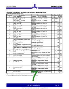
Switching Characteristics for ASM5P2304B Commercial Temperature Devices
Parameter
Description
Test Conditions
Min Typ Max Unit
1/t1
Output Frequency
30pF load, -1,-1H,-2, -2H devices
4
20 MHz
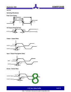
Duty Cycle 5= (t2 / t1) * 100
(-1, -2, -1H, -2H)
Measured at 1.4V, FOUT = 20MHz
40.0 50.0 60.0
45.0 50.0 55.0
%
%
30pF load
Duty Cycle 5 = (t2 / t1) * 100
(-1, -2,-1H, -2H)
Measured at 1.4V, FOUT = <20MHz
15pF load
Measured between 0.8V and 2.0V
Output Rise Time 5
(-1, -2)
t3
t3
t3
t4
t4
t4
2.20 nS
1.50 nS
1.50 nS
2.20 nS
1.50 nS
1.25 nS
30pF load
Output Rise Time 5
(-1, -2)
Measured between 0.8V and 2.0V
15pF load
Measured between 0.8V and 2.0V
Output Rise Time 5
(-1H, -2H)
30pF load
Output Fall Time 5
(-1, -2)
Measured between 2.0V and 0.8V
30pF load
Measured between 2.0V and 0.8V
Output Fall Time 5
(-1, -2)
15pF load
Output Fall Time 5
(-1H, -2H)
Measured between 2.0V and 0.8V
30pF load
Output-to-output skew on same bank
All outputs equally loaded
All outputs equally loaded
All outputs equally loaded
200
200
(-1, -2)
Output-to-output skew (-1H, -2H)
t5
pS
Output bank A -to- output bank B skew
200
(-1, -2H)
Output bank A to output bank b skew
(-2)
All outputs equally loaded
Measured at VDD /2
400
Delay, REF Rising Edge to FBK Rising
t6
t7
t8
0
0
±250 pS
Edge 5
Measured at VDD/2 on the FBK pins of
the device
Device-to-Device Skew 5
Output Slew Rate5
500
pS
Measured between 0.8V and 2.0V using
1
V/nS
Test Circuit #2
Measured at 20MHz, loaded outputs,
15pF load
175
200
100
400
375
1.0
Cycle-to-cycle jitter 5
(-1, -1H, -2H)
Measured at 20MHz, loaded outputs,
tJ
pS
30pF load
Measured at 20MHz, loaded outputs,
15pF load
Measured at 20MHz, loaded outputs,
Cycle-to-cycle jitter 5
(-2)
30pF load
tJ
pS
Measured at 20MHz, loaded outputs,
15pF load
Stable power supply, valid clock
tLOCK
PLL Lock Time 5
mS
presented on REF and FBK pins
Note:
5. Parameter is guaranteed by design and characterization. Not 100% tested in production.
3.3V Zero Delay Buffer
5 of 13
Notice: The information in this document is subject to change without notice.

 ALSC [ ALLIANCE SEMICONDUCTOR CORPORATION ]