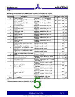
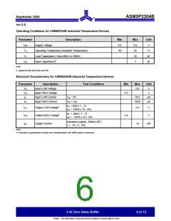
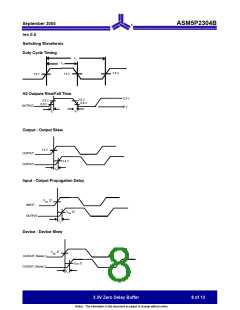
September 2005
ASM5P2304B
rev 0.5
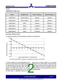
ASM5P2304B Configurations
Device
Feedback From
Bank A Frequency
Bank B Frequency
ASM5P2304B-1
ASM5P2304B-1H
ASM5P2304B-2
ASM5P2304B-2
ASM5P2304B-2H
ASM5P2304B-2H
Bank A or Bank B
Bank A or Bank B
Bank A
Reference
Reference
Reference
Reference
Reference
Reference /2
Reference
Bank B
2 X Reference
Reference
Bank A
Reference /2
Reference
Bank B
2 X Reference
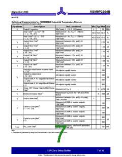
Zero Delay and Skew Control
For applications requiring zero input-output delay, all outputs must be equally loaded.
1500
1000
500
0
5
-30
30
-25
10
15
20
25
-20
-15
-10
-5
0
-500
-1000
-1500
Output Load Difference: FBK Load - CLKA/CLKB Load (pF)
REF Input to CLKA/CLKB Delay Vs Difference in Loading between FBK pin and CLKA/CLKB pins
To close the feedback loop of the ASM5P2304B, the FBK
pin can be driven from any of the four available output pins.
The output driving the FBK pin will be driving a total load of
7pF plus any additional load that it drives. The relative
loading of this output (with respect to the remaining
outputs) can adjust the input output delay. This is shown in
the above graph. For applications requiring zero input-
output delay, all outputs including the one providing
feedback should be equally loaded. If input-output delay
adjustments are required, use the above graph to calculate
loading differences between the feedback output and
remaining outputs. For zero output-output skew, be sure to
load outputs equally.
3.3V Zero Delay Buffer
2 of 13
Notice: The information in this document is subject to change without notice.

 ALSC [ ALLIANCE SEMICONDUCTOR CORPORATION ]