September 2005
rev 0.5
ASM5P2304B
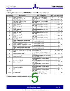
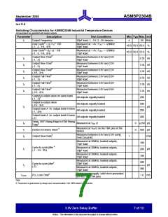
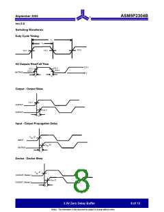
Switching Characteristics for ASM5I2304B Industrial Temperature Devices
All parameters are specified with loaded outputs
Parameter
Description
Test Conditions
Min Typ Max Unit
t1
Output Frequency
30pF load,-1, -1H,-2, -2H devices
4
20 MHz
Duty Cycle8 = (t2 / t1) * 100
(-1, -2, -1H, -2H)
Measured at 1.4V, FOUT = <20MHz
40.0 50.0 60.0
45.0 50.0 55.0
%
%
30pF load
Duty Cycle8= (t2 / t1) * 100
(-1, -2, -1H, -2H)
Measured at 1.4V, FOUT = <20MHz
15pF load
Measured between 0.8V and 2.0V
Output Rise Time8
(-1, -2)
t3
t3
t3
t4
t4
t4
2.50 nS
1.50 nS
1.50 nS
2.50 nS
1.50 nS
1.25 ns
200
30pF load
Output Rise Time8
(-1, -2)
Measured between 0.8V and 2.0V
15pF load
Measured between 0.8V and 2.0V
Output Rise Time8
(-1H, -2H)
30pF load
Output Fall Time8
(-1, -2)
Measured between 2.0V and 0.8V
30pF load
Measured between 2.0V and 0.8V
Output Fall Time8
(-1, -2)
15pF load
Output Fall Time8
(-1H, -2H)
Measured between 2.0V and 0.8V
30pF load
Output-to-output skew on same bank
All outputs equally loaded
All outputs equally loaded
All outputs equally loaded
All outputs equally loaded
Measured at VDD /2
(-1, -2)8
Output-to-output skew
(-1H, -2H)
Output bank A -to- output bank B skew
200
pS
200
t5
(-1, -2H)
Output bank A -to- output bank B skew
(-2)
Delay, REF Rising Edge to FBK Rising
400
t6
t7
t8
0
0
±250 pS
500 pS
V/nS
Edge8
Measured at VDD/2 on the FBK pins of the
device
Device-to-Device Skew 8
Output Slew Rate8
Measured between 0.8V and 2.0V using
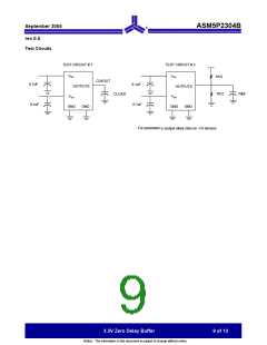
1
Test Circuit #2
Measured at 20MHz, loaded outputs,
15pF load
180
Cycle-to-cycle jitter 8
(-1, -1H, -2H)
Measured at 20MHz, loaded outputs,
tJ
pS
pS
200
100
400
380
30pF load
Measured at 20MHz, loaded outputs,
15pF load
Measured at 20MHz, loaded outputs,
Cycle-to-cycle jitter8
(-2)
30pF load
tJ
Measured at 20MHz, loaded outputs,
15pF load
Stable power supply, valid clock presented
tLOCK
PLL Lock Time8
1.0 mS
on REF and FBK pins
Note:
8. Parameter is guaranteed by design and characterization. Not 100% tested in production.
3.3V Zero Delay Buffer
7 of 13
Notice: The information in this document is subject to change without notice.

 ALSC [ ALLIANCE SEMICONDUCTOR CORPORATION ]