[ASAHI KASEI]
[AK7740ET]
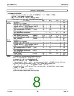
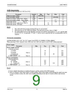
(2) DC characteristics
(VDD=AVDD=DVDD=3.0~3.6V,Ta=25°C)
Parameter
High level input voltage
Low level input voltage
Symbol
VIH
Min
80%VDD
Typ
Max
Unit
V
VIL
20%VDD
V
VOH
VDD-0.5
V
High level output voltage Iout=-100µA
Low level output voltage Iout=100µA
VOL
0.5
±10
V
Input leak current
Note 1)
Iin
Iid
Iix
µA
µA
µA
Input leak current (pull-down) Note 2)
Input leak current (XTI pin)
22
24
Note:
1. Pins with pull-down resistors and the XTI pin are not included
2. Pull-down pins are JX, SDIN and SDINA. The pull-down resistor value is 156kΩ
3. For input/output levels in this datasheet: the low level will be represented as "L" or 0, and the high
level as "H" or 1. In principle, "0" and "1" will be used to represent the bus (serial/parallel) such as
registers.
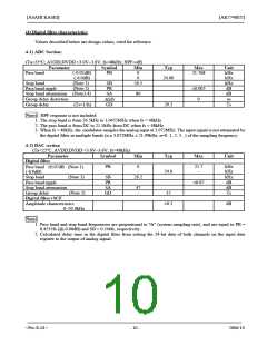
(3) Current consumption
(AVDD=DVDD=3.0V~3.6V, Ta=25°C; master clock (XTI)=24.576MHz=512fs[fs=48kHz];
When operating 4 DAC channels with a 1kHz sine wave full-scale input to each of ADC analog input pin)
Power supply
Parameter
Power supply current
Min
Typ
Max
Unit
1) During operation
a) AVDD
34
mA
b) DVDD
Note 1)
Note 2)
31
65
5
mA
mA
mA
c) Total (a+b)
90
2) INIT_RESET ="L"
Power consumption
1)During operation
a) AVDD
112
102
214
17
mW
mW
mW
mW
b) DVDD
Note 1)
Note 2)
c) Total (a+b)
2) INIT_RESET ="L"
324
Note:
1) Varies slightly depending on sampling frequency and the content of the DSP program.
2) This is a reference value when using a crystal oscillator. Most of the supply current during the initial reset state
is in the oscillator section; the value varies slightly depending on the type of crystal oscillator and external
circuit.
<Pre-E-01>
- 9 -
2006/10

 AKM [ ASAHI KASEI MICROSYSTEMS ]