[ASAHI KASEI]
[AK7740ET]
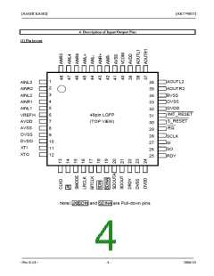
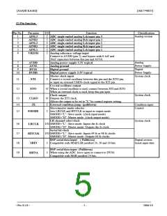
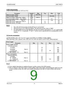
(2) Pin function
Pin No.
Pin name
AINL3
AINR2
AINL2
AINR1
AINL1
VREFH
I/O
Function
Classification
Analog section
1
2
3
4
5
6
I
I
I
I
I
I
ADC single-ended analog Lch input pin 3
ADC single-ended analog Rch input pin 2
ADC single-ended analog Lch input pin 2
ADC single-ended analog Rch input pin 1
ADC single-ended analog Lch input pin 1
Analog reference voltage input
Connect to AVDD (pin 7), and bypass with 0.1uF and
10uF capacitors between this pin and AVSS.
Analog power supply 3.3V typical
Analog ground
7
8
-
-
-
-
Analog
AVDD
AVSS
DVSS
DVDD
Power Supply
9
Digital
Digital ground
Power Supply
10
Digital power supply 3.3V typical
System clock
Master clock input
11
I Connect a crystal oscillator between this pin and the XTO pin,
or input an external CMOS clock signal to the XTI pin.
Crystal oscillator output
XTI
12
O When a crystal oscillator is used, connect between XTI and XTO.
When an external clock is used, keep this pin open
Clock output
XTO
System clock
13
14
15
O Outputs the XTI clock.
CLKO
JX
Allows the output to be set to "L" by control register setting.
I
I
Condition input
Control
External condition jump (pulldown)
Slave/master mode selector
SMODE
Sets LRCLK and BITCLK to input or output mode.
SMODE="L": Slave mode (clock input mode)
SMODE="H": Master mode (clock output mode)
LR channel select clock
System clock
16
17
18
19
I/O SMODE="L": Slave mode: Inputs the fs clock
SMODE="H": Master mode: Outputs the fs clock
Serial bit clock
I/O SMODE="L": Slave mode: Inputs 64 fs or 48 fs clocks
SMODE="H": Master mode: Outputs 64 fs clocks
DSP serial data input ( Pulldown)
LRCLK
BITCLK
SDIN
Digital section
I Compatible with MSB/LSB justified 24, 20 and 16 bits.
Serial input data
DSP serial data input (Pulldown)
I When using the ADC, leave open or connect to DVSS.
SDINA
Compatible with MSB justified 24 bits.
<Pre-E-01>
- 5 -
2006/10

 AKM [ ASAHI KASEI MICROSYSTEMS ]