[AK4679]
■ DSP STATE TRANSITION
The DSP blcok has follwing operating modes which are controlled by power supply, registors setting, program setting
and external clocks.
♦ Power Down (PDNE pin= “L”)
When the PDNE pin = “L” the DSP block is in powered-down state. Power supplies must be applied when the
PDNE pin = “L”. Set the PDNE pin to “H” to release the power-down after all power supplies are fed. More than
tPDNE cycle of “L” period is needed before releasing the power-down. The state moves the Hardware Reset
state by bringing the PDNE pin = “H”.
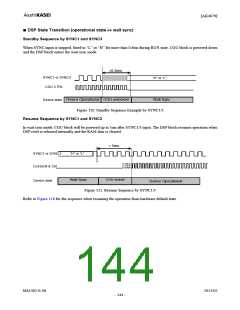
♦ Hardware Reset
The DSP is also in reset state in this mode. The clcocks and digital signals are bypassed to the output pins as
shown in Figure 109. The frame sync SYNC1 goes through SYNC2, and BCLK1 through BCLK2. The dital
signal path is shown in Figure 109. Do not apply a clock over 3.072MHz to the BCLK pin. In hardware reset
state, control registers (CONT0~8) cannot be accessed. The DSP block enters hardware suspended state when
the internal digital block is powered-up by setting the system power supply register (PCONT0: PWSW bit) to
“1”.
♦ Hardware Suspended
The power supply control block is initialized when the system power supply register (PCONT1: MRSTN bit) is
set to “1”. Control registers are reset and the DSP block goes into sleep state.
♦ Sleep (Standby)
In this state, all internal registers are in their default values. Register settings and DSP program downloading to
the RAM are available. TESTA, B, C bit, Digital I/F format and DSP related register settings should be made in
DSP reset state (DSPRSTN bit = “0”). CONT8 TESTC bit must be set to “1”. After these settings, set DLRDY
bit for the access pamission of internal memories to download DSP programs. The DLRDY bit must be cleared
after downloading DSP programs. Then, release the DSP reset (DSPRSTN bit = “1”). Clock inputs (BCLK1 or
3, SYNC1 or 3) are not necessary when writing to PRAM or CRAM.
♦ Wait Sync
After releasing DSP reset, DRAM and DLRAM data are cleared by “0” and the DSP block enters wait sync state.
In this state, the clock generator (CGU) is powered-up if an external clock is input to Port#1 or Port#3. Then the
DSP block enters normal operation mode after the output clock of CGU is stabilized. For a proper operation of
the system, a burst clock or a clock with two different frequencies locally are prohibited to use as BCLK or
SYNC. Uniform clocks must be input without a frequency deviation. In sleep mode, the CGU block does not
power up since an external clock cannot be received.
♦ DSP Operational (Run state)
The CGU block is powered-up when BCLK and SYNC clocks are detected in Wait Sync mode. The DSP block
becomes RUN state and CGU block starts to control clocks and DSP core.
The CGU block is unlocked when no input clocks are present during an operation and the DSP block enters
either Wait Sync state or Hardware Reset.
1. Wait Sync State
When the input clock at Port#1 or Port#3 is stopped for a certaion period (Figure 120), the DSP block
enters wait sync state. Registers, PRAM, CRAM and OFREG data are maintained. The CGU block is
in powere-down state until the clock is input again.
2. Hardware Reset State
When MRSTN bit = “0” and PWSW bit= “0”, the CGU block is powered-down and the internal
registers are initialized.The system power supply switch is turned off and PRAM, CRAM and
DLRAM are cleared. Regster values are also cleared to the default values. This mode is suitable for
standby in low power consumption. To resume the device operation, register settings and program
downloadings are necessary.
MS1402-E-06
2013/02
- 140 -

 AKM [ ASAHI KASEI MICROSYSTEMS ]