[AK4679]
MSBSA bit BCKPA bit
Data Interface Format
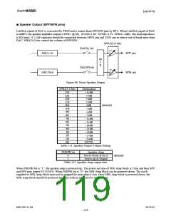
Figure
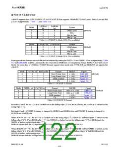
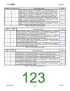
MSB of SDTOA is output by next rising edge (“↑”) of the falling edge (“↓”) of
BICKA after the rising edge (“↑”) of SYNCA. MSB of SDTIA is latched by the
falling edge (“↓”) of the BICKA just after the output timing of SDTOA’s MSB.
MSB of SDTOA is output by next falling edge (“↓”) of the rising edge (“↑”) of
BICKA after the rising edge (“↑”) of SYNCA. MSB of SDTIA is latched by the
rising edge (“↑”) of the BICKA just after the output timing of SDTOA’s MSB.
MSB of SDTOA is output by the 2nd rising edge (“↑”) of BICKA after the rising
edge (“↑”) of SYNCA. MSB of SDTIA is latched by the falling edge (“↓”) of the
BICKA just after the output timing of SDTOA’s MSB.
0
0
1
1
0
1
0
1
Figure 88
Figure 89
Figure 90
Figure 91
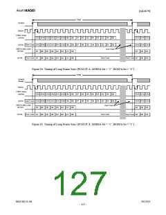
MSB of SDTOA is output by the 2nd falling edge (“↓”) of BICKA after the rising
edge (“↑”) of SYNCA. MSB of SDTIA is latched by the rising edge (“↑”) of the
BICKA just after the output timing of SDTOA’s MSB.
Table 119. PCM I/F A Format in Mode 0
MSBSB
bit
BCKPB
bit
Data Interface Format
Figure
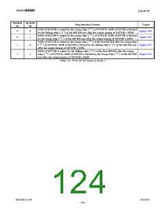
MSB of SDTOB is output by next rising edge (“↑”) of the falling edge (“↓”) of BICKB
after the rising edge (“↑”) of SYNCB. MSB of SDTIB is latched by the falling edge (“↓”) Figure 96
of the BICKB just after the output timing of SDTOB’s MSB.
MSB of SDTOB is output by next falling edge (“↓”) of the rising edge (“↑”) of BICKB
after the rising edge (“↑”) of SYNCB. MSB of SDTIB is latched by the rising edge (“↑”) Figure 97
of the BICKB just after the output timing of SDTOB’s MSB.
MSB of SDTOB is output by the 2nd rising edge (“↑”) of BICKB after the rising edge
(“↑”) of SYNCB. MSB of SDTIB is latched by the falling edge (“↓”) of the BICKB just Figure 98
after the output timing of SDTOB’s MSB.
0
0
1
1
0
1
0
1
MSB of SDTOB is output by the 2nd falling edge (“↓”) of BICKB after the rising edge
(“↑”) of SYNCB. MSB of SDTIB is latched by the rising edge (“↑”) of the BICKB just Figure 99
after the output timing of SDTOB’s MSB.
Table 120. PCM I/F B Format in Mode 0
MSBSA BCKPA
Data Interface Format
Figure
bit
bit
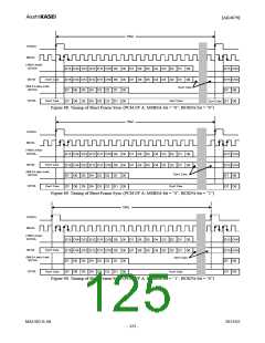
MSB of SDTOA is output by the rising edge (“↑”) of SYNCA. MSB of SDTIA is latched by
the falling edge (“↓”) of the BICKA just after the output timing of SDTOA’s MSB.
MSB of SDTOA is output by the rising edge (“↑”) of SYNCA. MSB of SDTIA is latched by
the rising edge (“↑”) of the BICKA just after the output timing of SDTOA’s MSB.
MSB of SDTOA is output by the rising edge (“↑”) of the first BICKA after the rising edge
(“↑”) of SYNCA. MSB of SDTIA is latched by the falling edge (“↓”) of the BICKA just
after the output timing of SDTOA’s MSB.
MSB of SDTOA is output by the falling edge (“↓”) of the first BICKA after the rising edge
(“↑”) of SYNCA. MSB of SDTIA is latched by the rising edge (“↑”) of the BICKA just
after the output timing of SDTOA’s MSB.
0
0
Figure 92
Figure 93
0
1
1
0
Figure 94
Figure 95
1
1
Table 121. PCM I/F A Format in Mode 1
MS1402-E-06
2013/02
- 123 -

 AKM [ ASAHI KASEI MICROSYSTEMS ]