[AK4679]
■ PCM I/F A & B Format
AK4679 supports dual PCM I/F (PCM I/F A & PCM I/F B) that supports 3 kind of I/F (16bit Linear, 8bit A-Law and 8bit
μ-Law) independently (Table 115 and Table 116).
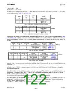
LAWA1
LAWA0
Mode
Format
bit
bit
0
1
2
3
0
0
1
1
0
1
0
1
16bit Linear
N/A
8bit A-Law
8bit μ-Law
(default)
(default)
Table 115. PCM I/F A Mode (N/A: Not available)
Mode
LAWB1 bit LAWB0 bit
Format
16bit Linear
N/A
8bit A-Law
8bit μ-Law
0
1
2
3
0
0
1
1
0
1
0
1
Table 116. PCM I/F B Mode (N/A: Not available)
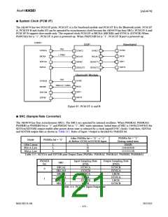
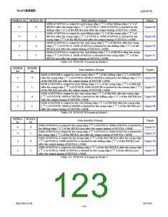
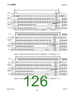
Four types of data formats are available and are selected by setting the FMTA1-0 and FMTB1-0 bits independently (Table
117 and Table 118). In 16bit Linear mode, the serial data is MSB first, 2’s complement format. In 8bit A-Law and μ-Law
Mode, the serial data is MSB first. PCM I/F formats support slave mode only. SYNCA/B and BICKA/B are input to the
AK4679.
Mode
FMTA1 bit FMTA0 bit
Format
Short Frame Sync
Long Frame Sync
MSB justified
I2S
BICKA
≥ 16fs2
≥ 16fs2
≥ 32fs2
≥ 32fs2
Figure
0
1
2
3
0
0
1
1
0
1
0
1
Table 119
Table 121
Figure 104
Figure 106
(default)
Table 117. PCM I/F A Format
Mode
FMTB1 bit FMTB0 bit
Format
Short Frame Sync
Long Frame Sync
MSB justified
I2S
BICKB
Figure
Table 120
Table 122
Figure 105
Figure 107
0
1
2
3
0
0
1
1
0
1
0
1
(default)
16fs3 or ≥ 32fs3
16fs3 or ≥ 32fs3
≥ 32fs3
≥ 32fs3
Table 118. PCM I/F B Format
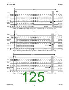
In modes 2 and 3, the SDTOA/B is clocked out on the falling edge (“↓”) of BICKA/B and the SDTIA/B is latched on the
rising edge (“↑”).
In Modes 0 and 1, PCM I/F A timing is changed by BCKPA and MSBSA bits, and PCM I/F B timing is changed by
BCKPB and MSBSB bits.
When BCKPA bit = “0”, the SDTOA is clocked out on the rising edge (“↑”) of BICKA and the SDTIA is latched on the
falling edge (“↓”). When BCKPA bit = “1”, the SDTOA is clocked out on the falling edge (“↓”) of BICKA and the
SDTIA is latched on the rising edge (“↑”).
MSBSA bit can shift the MSB position of SDTOA and SDTIA by half period of BICKA.
When BCKPB bit = “0”, the SDTOB is clocked out on the rising edge (“↑”) of BICKB and the SDTIB is latched on the
falling edge (“↓”). When BCKPB bit = “1”, the SDTOB is clocked out on the falling edge (“↓”) of BICKB and the
SDTIB is latched on the rising edge (“↑”).
MSBSB bit can shift the MSB position of SDTOB and SDTIB by half period of BICKB.
MS1402-E-06
2013/02
- 122 -

 AKM [ ASAHI KASEI MICROSYSTEMS ]