[AK4679]
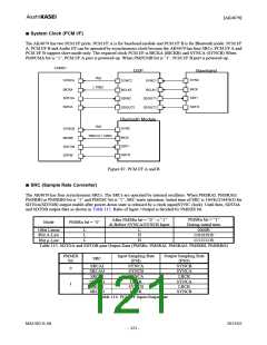
■ System Clock (PCM I/F)
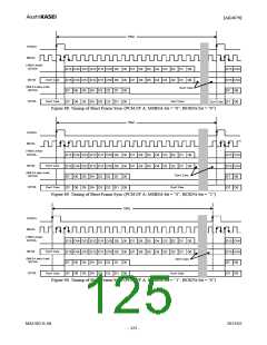
The AK4679 has two PCM I/F ports. PCM I/F A is for baseband module and PCM I/F B is for Bluetooth mode. PCM I/F
A, PCM I/F B and Audio I/F can be operated by asynchronous clock because the AK4679 has four SRCs. PCM I/F A and
PCM I/F B support slave mode only. The required clock PCM I/F is BICKA (BICKB) and SYNCA (SYNCB).When
PMPCMA bit is “1”, PCM I/F A port is powered-up. When PMPCMB bit is “1”, PCM I/F B port is powered-up.
CODEC
DSP
Baseband
1fs2
SYNC
SYNCA
SYNC2
SYNC1
≥ 16fs2
BICK
SDTI
BICKA
SDTOA
SDTIA
BCLK2
SDIN2
BCLK1
SDOUT1
SDTO
SDOUT2
SDOUT2
Bluetooth Module
1fs3
SYNC
SYNCB
16fs3 or ≥ 32fs3
BICK
SDTI
SDTO
BICKB
SDTOB
SDTIB
Figure 87. PCM I/F A and B
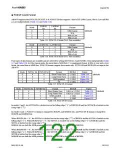
■ SRC (Sample Rate Converter)
The AK4679 has four asynchronous SRCs. The SRCs are operated by internal oscillator. When PMSRAI, PMSRAO,
PMSRBI or PMSRBO bit is “1” and PMOSC bit is “1”, SRC starts operation. Initial time of SRC is 164/fs2(164/fs3) for
SDTOA(SDTOB) output enable after power-down state is released by a clock input(SYNC clock). Until then, SDTOA
and SDTOB output data as shown in Table 113. Ratio of Input / Output is decided by PMMIX bit.
PMSRx bit = “1”
During initial time
After PMSRx bit = “0” → “1”
& Before SYNCA/SYNCB Input
Mode
PMSRx bit = “0”
16bit Linear
8bit A-Law
8bit μ-Law
L
L
L
L
H
H
0000H
11010101b
11111111b
Table 113. SDTOA and SDTOB pins Output Data (PMSRx: PMSRAI, PMSRAO, PMSRBI, PMSRBO)
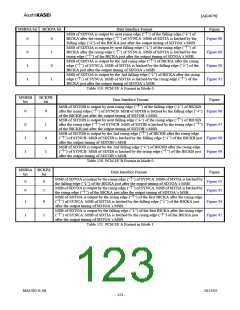
PMMIX
bit
Input Sampling Rate
(FSI)
Output Sampling Rate
(FSO)
SRC
SRCAI
SRCAO
SRCAI
SRCAO
SRCBI
SRCBO
SYNCA
SYNCB
SYNCA
LRCK
SYNCB
LRCK
SYNCB
SYNCA
LRCK
SYNCA
LRCK
SYNCB
0
1
Table 114. PCM I/F Input Output rate
MS1402-E-06
2013/02
- 121 -

 AKM [ ASAHI KASEI MICROSYSTEMS ]