[AK4679]
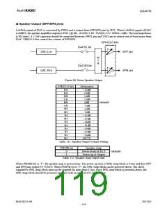
■ Speaker Output (SPP/SPN pins)
Lch/Rch signal of DAC is converted by PWM and is output from SPP/SPN pins by BTL. When Lch/Rch signal of DAC
is 0dBFS, the speaker amplifier outputs 0.89W ( @ 8Ω, AVDD=1.8V, SVDD=4.2V, SPKG=-6dB). The load impedance
is 8Ω (min). A 2.2nF capacitor should be connected between SPFIL pin and VSS1 pin to reduce out-of-band noise from
DAC. SPKG3-0 bits control the volume of SPP/SPN.
SPKG3-0 bits
DACSL bit
DAC Lch
DAC Rch
SPP pin
SPN pin
M
I
X
DACSR bit
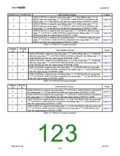
Figure 86. Mono Speaker Output
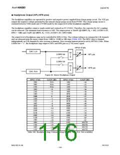
SPKG3-0 bits
Attenuation
+12dB
+9dB
FH
EH
DH
CH
BH
AH
9H
8H
7H
6H
5H
4H
3H
2H
1H
0H
+6dB
+3dB
0dB
−3dB
−6dB
−9dB
−12dB
−15dB
−18dB
−21dB
−24dB
−27dB
−30dB
MUTE
(default)
Table 111. Speaker Output Volume Setting
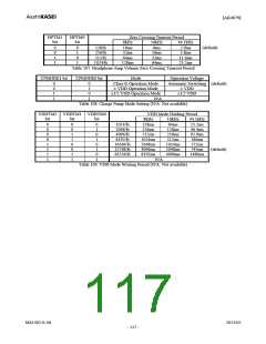
PMSPK bit
Speaker-Amp
0
1
Power-down & Hi-Z
Power-up & Output
(default)
Table 112. Speaker-Amp output state
When PMSPK bit is “1”, the speaker-amp is powered-up. The power-up time of SPK-Amp block is 32ms and then SPP
and SPN pins output 0V (VSS3). When PMSPK bit is “0”, the SPK-Amp block can be powered-down. The clock
supplied to SPK-Amp block must not be stopped for more than 0.5ms. Once SPK-Amp block is powered-down, the
SPK-Amp block should be powered-up again with an interval of 0.5ms or more.
MS1402-E-06
2013/02
- 119 -

 AKM [ ASAHI KASEI MICROSYSTEMS ]