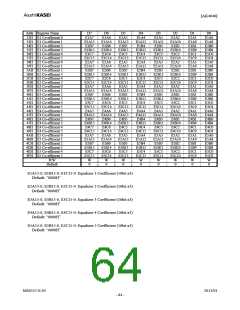
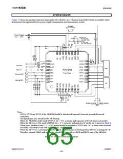
[AK4646]
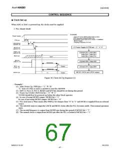
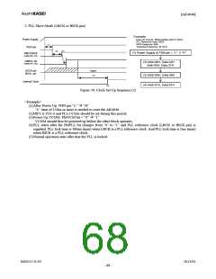
2. PLL Slave Mode (LRCK or BICK pin)
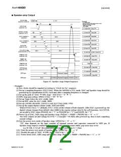
Example:
Audio I/F Format : MSB justified (ADC & DAC)
PLL Reference clock: BICK
Power Supply
BICK frequency: 64fs
(1)
Sampling Frequency: 44.1kHz
PDN pin
(2)
(3)
4fs of
(1) Power Supply & PDN pin = “L” Æ “H”
PMVCM bit
(Addr:00H, D6)
PMPLL bit
(Addr:01H, D0)
(2) Addr:04H, Data:32H
Addr:05H, Data:27H
LRCK pin
BICK pin
Input
(4)
(3) Addr:00H, Data:40H
(4) Addr:01H, Data:01H
Internal Clock
(5)
Figure 39. Clock Set Up Sequence (2)
<Example>
(1)After Power Up: PDN pin “L” Æ “H”
“L” time of 150ns or more is needed to reset the AK4646.
(2)DIF1-0, FS3-0 and PLL3-0 bits should be set during this period.
(3)Power Up VCOM: PMVCM bit = “0” Æ “1”
VCOM should first be powered up before the other block operates.
(4)PLL starts after the PMPLL bit changes from “0” to “1” and PLL reference clock (LRCK or BICK pin) is
supplied. PLL lock time is 160ms (max) when LRCK is a PLL reference clock. And PLL lock time is 2ms (max)
when BICK is a PLL reference clock.
(5)Normal operation stats after that the PLL is locked.
MS0557-E-05
2011/01
- 68 -

 AKM [ ASAHI KASEI MICROSYSTEMS ]