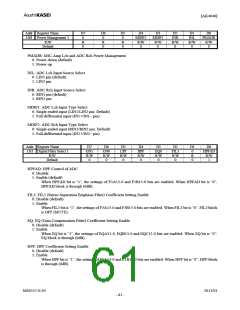
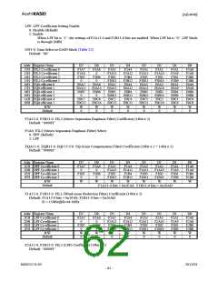
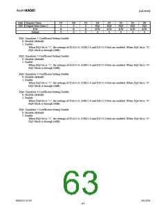
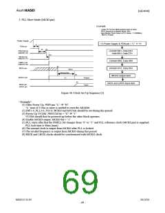
[AK4646]
SYSTEM DESIGN
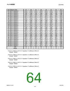
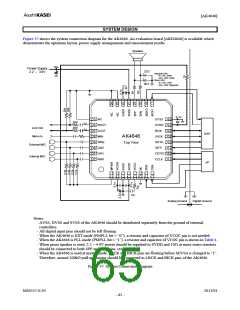
Figure 37 shows the system connection diagram for the AK4646. An evaluation board [AKD4646] is available which
demonstrates the optimum layout, power supply arrangements and measurement results.
Speaker
10u
Power Supply
ZD2
2.2 ∼ 3.6V
Dynamic SPK
R1, R2: Short
ZD1, ZD2: Open
Piezo SPK
R1, R2: ≥10Ω
ZD1, ZD2: Required
ZD 1
0.1u
NC
DVSS
DVDD
BICK
25
26
16
15
14
200
200
1u
1u
ROUT
Line Out
Mono In
27 LOUT
28 MIN
DSP
LRCK 13
SDTO 12
AK4646
Top View
29 RIN2
External MIC
LIN2
LIN1
SDTI
30
31
11
10
9
CDTIO
CCLK
Internal MIC
32 RIN1
μP
Cp
Digital Ground
Analog Ground
Notes:
- AVSS, DVSS and SVSS of the AK4646 should be distributed separately from the ground of external
controllers.
- All digital input pins should not be left floating.
- When the AK4646 is EXT mode (PMPLL bit = “0”), a resistor and capacitor of VCOC pin is not needed.
- When the AK4646 is PLL mode (PMPLL bit = “1”), a resistor and capacitor of VCOC pin is shown in Table 4.
- When piezo speaker is used, 2.2 ∼ 4.0V power should be supplied to SVDD and 10Ω or more series resistors
should be connected to both SPP and SPN pins, respectively.
- When the AK4646 is used at master mode, LRCK and BICK pins are floating before M/S bit is changed to “1”.
Therefore, around 100kΩ pull-up resistor should be connected to LRCK and BICK pins of the AK4646.
Figure 37. System Connection Diagram
MS0557-E-05
2011/01
- 65 -

 AKM [ ASAHI KASEI MICROSYSTEMS ]