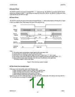
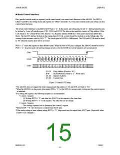
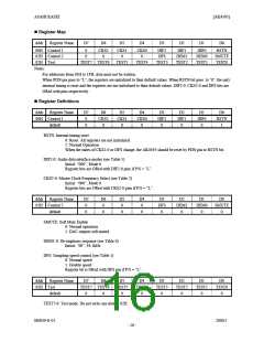
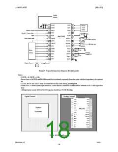
ASAHI KASEI
[AK4393]
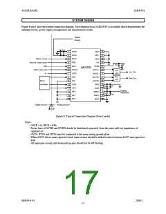
1. Grounding and Power Supply Decoupling
To minimize coupling by digital noise, decoupling capacitors should be connected to AVDD and DVDD, respectively.
AVDD is supplied from analog supply in system and DVDD is supplied from digital supply in system. If AVDD and
DVDD are supplied separately, the power up sequence is not critical. AVSS, BVSS and DVSS must be connected
to analog ground plane. System analog ground and digital ground should be connected together near to where the
supplies are brought onto the printed circuit board. Decoupling capacitors for high frequency should be placed as near as
possible.
2. Voltage Reference
The differential Voltage between VREFH and VREFL set the analog output range. VREFH pin is normally connected to
AVDD and VREFL pin is normally connected to AVSS. VREFH and VREFL should be connected with a 0.1µF ceramic
capacitor. VCOM is a signal ground of this chip. An electrolytic capacitor 10µF parallel with a 0.1µF ceramic capacitor
attached to VCOM pin eliminates the effects of high frequency noise. No load current may be drawn from VCOM pin. All
signals, especially clocks, should be kept away from the VREFH, VREFL and VCOM pins in order to avoid unwanted
coupling into the AK4393.
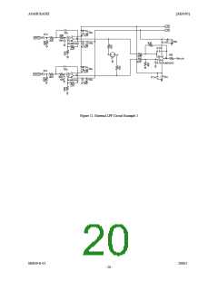
3. Analog Outputs
The analog outputs are full differential outputs and 2.4Vpp (typ@VREF=5V) centered around VCOM. The differential
outputs are summed externally, VAOUT = (AOUT+) - (AOUT-) between AOUT+ and AOUT-. If the summing gain is 1, the
output range is 4.8Vpp (typ@VREF=5V). The bias voltage of the external summing circuit is supplied externally. The
input data format is 2's complement. The output voltage (VAOUT) is a positive full scale for 7FFFFFH (@24bit) and a
negative full scale for 800000H (@24bit). The ideal VAOUT is 0V for 000000H(@24bit).
The internal switched-capacitor filters attenuate the noise generated by the delta-sigma modulator beyond the audio
passband.
Figure 11 shows an example of external LPF circuit summing the differential outputs by an op-amp.
Figure 12 shows an example of differential outputs and LPF circuit example by three op-amps.
AK4393
1k
1k
1k
AOUT-
1k
1k
1n
+Vop
3.3n
1k
Analog
Out
AOUT+
-Vop
1n
Figure 11. External LPF Circuit Example 1
M0039-E-01
2000/5
- 19 -

 AKM [ ASAHI KASEI MICROSYSTEMS ]