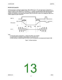
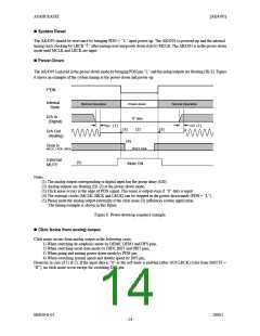
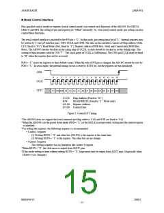
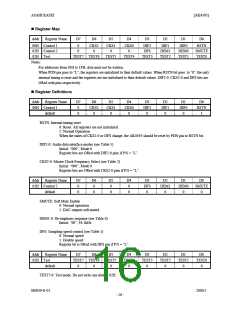
ASAHI KASEI
[AK4393]
SYSTEM DESIGN
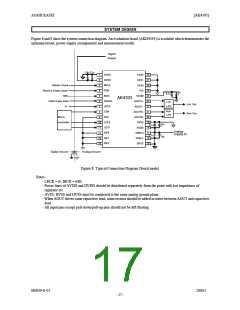
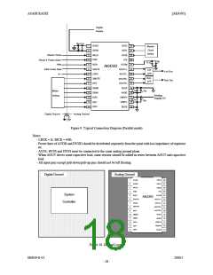
Figure 8 and 9 show the system connection diagram. An evaluation board (AKD4393) is available which demonstrates the
optimum layout, power supply arrangements and measurement results.
Digital
Supply
10u 0.1u
DVSS
DVDD
MCLK
PDN
CKS2 28
CKS1 27
CKS0 26
P/S 25
1
2
3
4
5
6
7
8
9
+
Master Clock
Reset & Power down
10u
+
0.1u
64fs
24bit Audio Data
fs
BICK
VCOM 24
AOUTL+ 23
AK4393
SDATA
LRCK
CSN
Lch
Lch Out
Rch Out
LPF
AOUTL-
22
21
Rch
LPF
AOUTR+
Micro-
AOUTR- 20
AVSS 19
DFS
controller
10 CCLK
11 CDTI
10u
+
0.1u
18
AVDD
Analog
Supply 5V
DIF0
12
13
14
VREFH 17
0.1u
VREFL 16
+
10u
DIF1
DIF2
BVSS 15
Digital Ground
Analog Ground
Figure 8. Typical Connection Diagram (Serial mode)
Notes:
- LRCK = fs, BICK = 64fs.
- Power lines of AVDD and DVDD should be distributed separately from the point with low impedance of
regulator etc.
- AVSS, BVSS and DVSS must be connected to the same analog ground plane.
- When AOUT drives some capacitive load, some resistor should be added in series between AOUT and capacitive
load.
- All input pins except pull-down/pull-up pins should not be left floating.
M0039-E-01
2000/5
- 17 -

 AKM [ ASAHI KASEI MICROSYSTEMS ]