ASAHI KASEI
[AK4393]
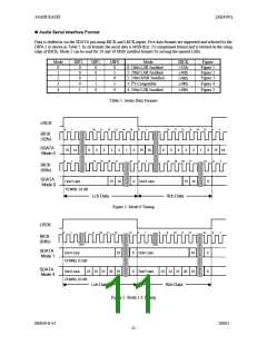
n Mode Control Interface
Pins (parallel control mode) or registers (serial control mode) can control each functions of the AK4393. For DIF2-0,
CKS2-0 and DFS, the setting of pin and register are “ORed” internally. So, even serial control mode, pin setting can also
control these functions.
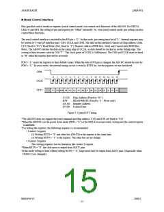
The serial control interface is enabled by the P/S pin = “L”. In this mode, pin setting must be all “L”. Internal registers may
be written by 3-wire µP interface pins: CSN, CCLK and CDTI. The data on this interface consists of Chip address (2bits,
C1/0; fixed to “01”), Read/Write (1bit; fixed to “1”), Register address (MSB first, 5bits) and Control data (MSB first,
8bits). The AK4393 latches the data on the rising edge of CCLK, so data should be clocked in on the falling edge. The
writing of data becomes valid by CSN “”. The clock speed of CCLK is 5MHz(max). The CSN and CCLK must be fixed
to “H” when the register does not be accessed.
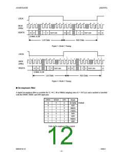
PDN = “L” resets the registers to their default values. When the state of P/S pin is changed, the AK4393 should be reset by
PDN = “L”. In serial mode, the internal timing circuit is reset by RSTN bit, but the registers are not initialized.
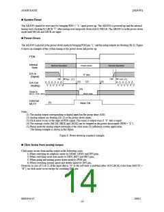
CSN
0
1
2
3
4
5
6
7
8
9
10 11 12 13 14 15
CCLK
CDTI
C1 C0 R/W A4 A3 A2 A1 A0 D7 D6 D5 D4 D3 D2 D1 D0
C1-C0: Chip Address (Fixed to “01”)
R/W:
READ/WRITE (Fixed to “1”, Write only)
A4-A0: Register Address
D7-D0: Control Data
Figure 7. Control I/F Timing
*The AK4393 does not support the read command and chip address. C1/0 and R/W are fixed to “011”
*When the AK4393 is in the power down mode (PDN = “L”) or the MCLK is not provided, writing into the control register
is inhibited.
*For setting the registers, the following sequence is recommended.
Control 1 register
(1) Writing RSTN = “0” and other bits (D6-D1) to the register at the same time.
(2) Writing RSTN = “1” to the register. The other bits are no change.
Control 2 register
This writing sequence has no limitation like control 1 register.
*When RSTN = “0”, the click noise is output from AOUT pins.
*If the mode setting is done without setting RSTN = “0”, large noise may be output from AOUT pins. (Especially when
CKS0/1/2 are changed.)
M0039-E-01
2000/5
- 15 -

 AKM [ ASAHI KASEI MICROSYSTEMS ]