ASAHI KASEI
[AK4393]
Digital
Supply
10u 0.1u
+
DVSS
CKS2 28
CKS1 27
CKS0 26
P/S 25
1
2
3
4
5
6
7
8
9
Master
Clock
DVDD
MCLK
PDN
Select
Master Clock
Reset & Power down
10u
+
0.1u
64fs
24bit Audio Data
fs
BICK
VCOM 24
AOUTL+ 23
AOUTL- 22
AK4393
SDATA
LRCK
SMUTE
DFS
Lch
Lch Out
LPF
Rch
LPF
AOUTR+
21
Rch Out
AOUTR- 20
AVSS 19
10 DEM0
11 DEM1
0.1u
18
Mode
10u
+
AVDD
setting
Analog
Supply 5V
DIF0
12
13
14
VREFH
17
0.1u
+
10u
VREFL 16
DIF1
DIF2
BVSS 15
Digital Ground
Analog Ground
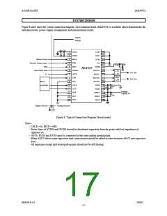
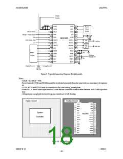
Figure 9. Typical Connection Diagram (Parallel mode)
Notes:
- LRCK = fs, BICK = 64fs.
- Power lines of AVDD and DVDD should be distributed separately from the point with low impedance of regulator
etc.
- AVSS, BVSS and DVSS must be connected to the same analog ground plane.
- When AOUT drives some capacitive load, some resistor should be added in series between AOUT and capacitive
load.
- All input pins except pull-down/pull-up pins should not be left floating.
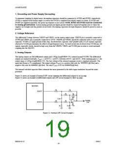
Digital Ground
Analog Ground
CKS2 28
CKS1 27
CKS0 26
P/S 25
1
2
3
4
5
6
7
8
9
DVSS
DVDD
MCLK
PDN
System
Controller
BICK
VCOM 24
AOUTL+ 23
AOUTL- 22
AK4393
SDATA
LRCK
SMUTE
AOUTR+
AOUTR-
21
20
DFS
10 DEM0
11 DEM1
AVSS 19
AVDD
18
17
DIF0
12
13
14
VREFH
VREFR 16
BVSS 15
DIF1
DIF2
Figure 10. Ground Layout
M0039-E-01
2000/5
- 18 -

 AKM [ ASAHI KASEI MICROSYSTEMS ]