ASAHI KASEI
[AK4393]
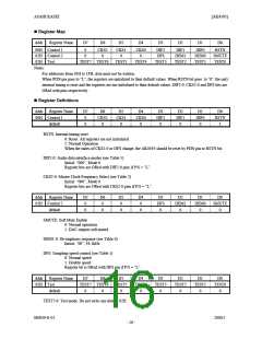
n Register Map
Addr
Register Name
D7
D6
D5
D4
D3
D2
D1
D0
00H Control 1
01H Control 2
02H Test
0
0
CKS2
0
CKS1
0
CKS0
0
DIF2
DFS
DIF1
DEM1
TEST2
DIF0
DEM0
TEST1
RSTN
SMUTE
TEST0
TEST7 TEST6
TEST5
TEST4
TEST3
Notes:
For addresses from 03H to 1FH, data must not be written.
When PDN pin goes to “L”, the registers are initialized to their default values. When RSTN bit goes to “0”, the only
internal timing is reset and the registers are not initialized to their default values. DIF2-0, CKS2-0 and DFS bits are
ORed with pins respectively.
n Register Definitions
Addr
Register Name
D7
0
D6
CKS2
0
D5
CKS1
0
D4
CKS0
0
D3
DIF2
0
D2
DIF1
0
D1
DIF0
0
D0
RSTN
1
00H Control 1
default
0
RSTN: Internal timing reset
0: Reset. All registers are not initialized.
1: Normal Operation
When the states of CKS2-0 or DFS change, the AK4393 should be reset by PDN pin or RSTN bit.
DIF2-0: Audio data interface modes (see Table 5)
Initial: “000”, Mode 0
Register bits are ORed with DIF2-0 pins if P/S = “L”.
CKS2-0: Master Clock Frequency Select (see Table 2)
Initial: “000”, Mode 0
Register bits are ORed with CKS2-0 pins if P/S = “L”.
Addr
Register Name
D7
0
D6
0
D5
0
D4
0
D3
DFS
0
D2
DEM1
0
D1
DEM0
0
D0
SMUTE
0
01H Control 2
default
0
0
0
0
SMUTE: Soft Mute Enable
0: Normal operation
1: DAC outputs soft-muted
DEM1-0: De-emphasis response (see Table 6)
Initial: “00”, 44.1kHz
DFS: Sampling speed control (see Table 1)
0: Normal speed
1: Double speed
Register bit is ORed with DFS pin if P/S = “L”.
Addr
02H Test
default
Register Name
D7
D6
D5
TEST5
0
D4
TEST4
0
D3
TEST3
0
D2
TEST2
0
D1
TEST1
0
D0
TEST0
0
TEST7 TEST6
0
0
TEST7-0: Test mode. Do not write any data to 02H.
M0039-E-01
2000/5
- 16 -

 AKM [ ASAHI KASEI MICROSYSTEMS ]