ASAHI KASEI
[AK4115]
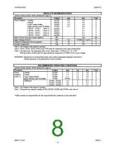
ABSOLUTE MAXIMUM RATINGS
(AVSS, OVSS, DVSS, TVSS, BVSS=0V; Note 2)
Parameter
Symbol
min
max
Units
Power Supplies: Analog
Digital
AVDD
DVDD
OVDD
TVDD
∆GND1
∆GND2
∆GND3
∆GND4
IIN
-0.3
-0.3
-0.3
-0.3
-
-
-
4.6
4.6
4.6
6.0
0.3
0.3
0.3
0.3
V
V
V
V
V
V
V
V
Logic Output Buffer
Input tolerance and TX Buffer
| BVSS – AVSS | (Note 3)
| BVSS – OVSS | (Note 3)
| BVSS – DVSS | (Note 3)
| BVSS – TVSS |
(Note 3)
-
-
Input Current (Any pins except supplies)
Input Voltage (Note 4)
Ambient Temperature (Power applied)
Storage Temperature
mA
V
±10
VIN
Ta
Tstg
-0.3
-20
-65
“TVDD+0.3” or 6.0
85
150
C
°
°C
Note 2. All voltages with respect to ground.
Note 3. AVSS, OVSS, DVSS, BVSS and TVSS must be connected to the same ground plane.
Note 4. All input pins. The maximum value is low value either “TVDD+0.3V” or “6.0V”.
Pull-up resistor at SDA and SCL pins should be connected to (TVDD+0.3)V or less voltage.
WARNING: Operation at or beyond these limits may result in permanent damage to the device.
Normal operation is not guaranteed at these extremes.
RECOMMENDED OPERATING CONDITIONS
(AVSS, OVSS, DVSS, TVSS, BVSS=0V; Note 2)
Parameter
Symbol
min
typ
max
Units
Power
Supplies:
(Note 5)
Analog
Digital
AVDD
DVDD
OVDD
2.7
2.7
2.7
DVDD
-0.3
3.3
3.3
3.3
5.0
0
3.6
3.6
3.6
5.5
0.3
0.3
0.3
V
V
V
V
V
V
V
Logic Output Buffer
Input tolerance and TX Buffer
Difference
TVDD
AVDD – DVDD
AVDD – OVDD
OVDD – DVDD
-0.3
-0.3
0
0
Note 2. All voltages with respect to ground.
Note 5. The power up sequence among AVDD, DVDD, OVDD and TVDD is not critical.
*AKM assumes no responsibility for the usage beyond the conditions in this data sheet.
MS0573-E-00
2006/12
- 8 -

 AKM [ ASAHI KASEI MICROSYSTEMS ]