ASAHI KASEI
[AK4115]
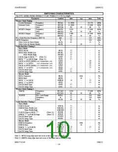
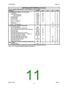
SWITCHING CHARACTERISTICS (Continued)
(Ta=25°C; AVDD, OVDD, DVDD=2.7~3.6V, TVDD=2.7~5.5V; CL=20pF)
Parameter
Symbol
min
typ
max
Units
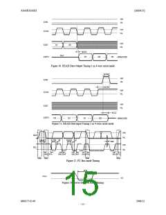
Control Interface Timing (4-wire serial mode)
CCLK Period
tCCK
tCCKL
tCCKH
tCDS
tCDH
tCSW
tCSS
tCSH
tDCD
tCCZ
200
80
80
50
50
150
50
50
-
-
-
-
-
-
-
-
-
-
-
-
-
-
-
-
-
-
-
45
ns
ns
ns
ns
ns
ns
ns
ns
ns
ns
CCLK Pulse Width Low
Pulse Width High
CDTI Setup Time
CDTI Hold Time
CSN “H” Time
CSN “↓” to CCLK “↑”
CCLK “↑” to CSN “↑”
CDTO Delay
-
70
CSN “↑” to CDTO Hi-Z
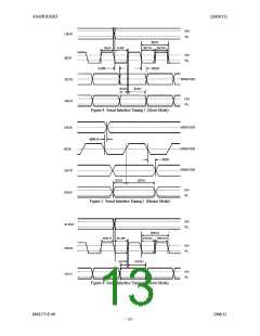
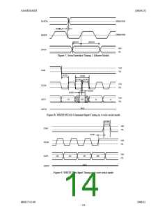
Control Interface Timing (I2C Bus mode):
SCL Clock Frequency
fSCL
tBUF
-
1.3
0.6
1.3
0.6
0.6
0
0.1
-
-
-
-
-
-
-
-
-
-
-
-
-
-
-
400
-
-
-
-
-
-
-
0.3
0.3
-
400
50
kHz
s
µ
s
µ
Bus Free Time Between Transmissions
Start Condition Hold Time (prior to first clock pulse)
Clock Low Time
Clock High Time
Setup Time for Repeated Start Condition
tHD:STA
tLOW
tHIGH
tSU:STA
tHD:DAT
tSU:DAT
tR
µs
µs
µs
µs
µs
SDA Hold Time from SCL Falling
SDA Setup Time from SCL Rising
Rise Time of Both SDA and SCL Lines
Fall Time of Both SDA and SCL Lines
Setup Time for Stop Condition
Capacitive load on bus
(Note 13)
s
µ
s
µ
tF
µs
pF
ns
tSU:STO
Cb
0.6
-
0
Pulse Width of Spike Noise Suppressed by Input Filter
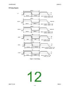
Reset Timing
PDN Pulse Width
tSP
tPW
150
-
-
ns
Note 13. Data must be held for sufficient time to bridge the 300ns transition time of SCL.
Note 14. I2C is a registered tradmark of Philips Semiconductors.
MS0573-E-00
2006/12
- 11 -

 AKM [ ASAHI KASEI MICROSYSTEMS ]