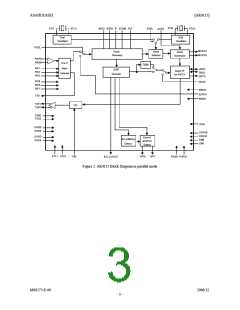
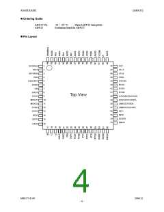
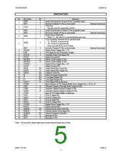
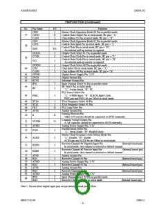
ASAHI KASEI
[AK4115]
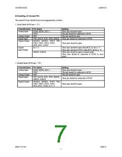
Handling of Unused Pin
The unused I/O pin should be processed appropriately as below.
1. Serial Mode (P/SN pin = “L”)
Classification Pin Name
Setting
Analog Input
RXP0, RXN0, RX7-1
These pins should be open.
TEST
This pin should be connected to AVSS.
Analog Output
Digital Input
FILT
This pin should be open.
These pin should be connected to DVSS.
VIN, DAUX, XTI1, XTI2, EMCK
Digital Output
MCKO1, MCKO2, VOUT, TX0,
TXP1, TXN1, XTO1, XTO2,
INT0, INT1, CDTO
These pins should be open.
Digital
Input/Output
B, U, C
These pins should be open when BCU_IC bit is “1”.
These pins should be DVSS when BCU_IO bit is “0”.
These pins should be open in master mode.
These pins should be connected to DVSS in slave
mode.
EBICK, ELRCK
2. Parallel Mode (P/SN pin = “H”)
Classification Pin Name
Setting
Analog Input
RXP0, RXN0, RX3-1
TEST
FILT
VIN, DAUX, XTI1, XTI2, EMCK,
EBICK, ELRCK
These pins should be open.
This pin should be connected to AVSS.
This pin should be open.
Analog Output
Digital Input
These pin should be connected to DVSS.
Digital Output
MCKO1, MCKO2, VOUT, TX0,
TXP1, TXN1, XTO1, XTO2,
INT0, INT1, CDTO, B, U, C
These pins should be open.
MS0573-E-00
2006/12
- 7 -

 AKM [ ASAHI KASEI MICROSYSTEMS ]