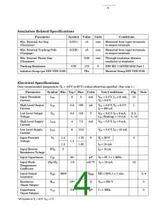
5
Switching Specifications
Over recommended temperature (TA = -40°C to 85°C), VCC = 5 V, IF = 7.5 mA unless otherwise specified.
Device
Parameter Symbol HCPL- Min. Typ.* Max. Unit
Test Conditions
Fig. Note
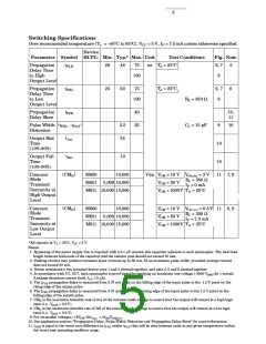
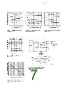
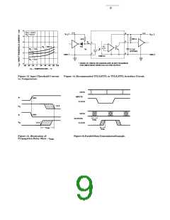
Propagation
Delay Time
to High
tPLH
tPHL
tPSK
20
25
48
50
75
ns TA = 25°C
6, 7
5
6
100
8
Output Level
Propagation
Delay Time
to Low
75
TA = 25°C
6, 7
8
100
RL = 350 Ω
Output Level
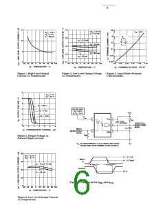
Propagation
Delay Skew
40
35
10,
11
Pulse Width |tPHL - tPLH
Distortion
|
3.5
24
CL = 15 pF
9
10
Output Rise
Time
(10%-90%)
trise
10
10
Output Fall
Time
tfall
10
(10%-90%)
Common
Mode
Transient
Immunity at
High Output
Level
|CMH|
M600
10,000
V/µs VCM = 10 V VO(min) = 2 V
11 7, 9
RL = 350 Ω
IF = 0 mA
M601 5,000 10,000
M611 10,000 15,000
VCM = 50 V
VCM =1000V TA = 25°C
Common
Mode
Transient
Immunity at
Low Output
Level
|CMH|
M600
10,000
VCM = 10 V VO(max) = 0.8 V 11 8, 9
RL = 350 Ω
IF = 7.5 mA
M601 5,000 10,000
M611 10,000 15,000
VCM = 50 V
VCM = 1000V
TA = 25°C
*All typicals at TA = 25°C, VCC = 5 V.
Notes:
1. Bypassing of the power supply line is required with a 0.1 µF ceramic disc capacitor adjacent to each optocoupler. The total lead
length between both ends of the capacitor and the isolator pins should not exceed 10 mm.
2. Peaking circuits may produce transient input currents up to 50 mA, 50 ns maximum pulse width, provided average current
does not exceed 20 mA.
3. Device considered a two terminal device: pins 1 and 3 shorted together, and pins 4, 5 and 6 shorted together.
4. In accordance with UL 1577, each optocoupler is proof tested by applying an insulation test voltage ≥ 3000 VRMS for 1 second
(Leakage detection current limit, II-O ≤ 5 µA).
5. The tPLH propagation delay is measured from 3.75 mA point on the falling edge of the input pulse to the 1.5 V point on the
rising edge of the output pulse.
6. The tPHL propagation delay is measured from 3.75 mA point on the rising edge of the input pulse to the 1.5 V point on the
falling edge of the output pulse.
7. CMH is the maximum tolerable rate of rise of the common mode voltage to assure that the output will remain in a high logic
state (i.e., VOUT > 2.0 V).
8. CML is the maximum tolerable rate of fall of the common mode voltage to assure that the output will remain in a low logic
state (i.e., VOUT > 0.8 V).
9. For sinusoidal voltages, (|dVCM|/dt)max = πfCMVCM(p-p)
.
10. See application section; “Propagation Delay, Pulse-Width Distortion and Propagation Delay Skew” for more information.
11. tPSK is equal to the worst case difference in tPHL and/or tPLH that will be seen between units at any given temperature within
the worst case operating condition range.

 AGILENT [ AGILENT TECHNOLOGIES, LTD. ]