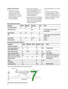
AC Electrical Specifications
Electrical Characteristics over recommended operating conditions. Typical values at 25 °C, V =2.6V.
DD3
Notes
Parameter
Symbol
Minimum Typical Maximum Units
From SW_RESET register write to valid
motion, assuming motion is present
Motion delay after reset tMOT-RST
23
50
ms
From STDWN pin active to low current
Shutdown
tSTDWN
ms
s
From STDWN pin inactive to valid
motion. Notes: A RESET must be
asserted after a shutdown. Refer to
section "Notes on Shutdown and
Forced Rest", also note tMOT-RST
Wake from shutdown
tWAKEUP
1
From RESTEN bits set to low current
Forced Rest enable
tREST-EN
1
1
s
s
From RESTEN bits cleared to valid
motion
Wake from Forced Rest tREST-DIS
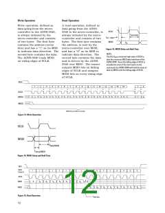
CL = 100pF
CL = 100pF
MISO rise time
tr-MISO
150
150
300
300
120
ns
ns
ns
MISO fall time
tf-MISO
From SCLK falling edge to MISO data
valid, no load conditions
MISO delay after SCLK
tDLY-MISO
Data held until next falling SCLK edge
MISO hold time
MOSI hold time
tHOLD-MISO
tHOLD-MOSI
0.5
1/fSCLK
µs
ns
Amount of time data is valid after SCLK
rising edge
200
From data valid to SCLK rising edge
MOSI setup time
tSETUP-MOSI 120
ns
From rising SCLK for last bit of the first
data byte, to rising SCLK for last bit of
the second data byte.
SPI time between write tSWW
commands
30
µs
From rising SCLK for last bit of the first
data byte, to rising SCLK for last bit of
the second address byte.
SPI time between write tSWR
and read commands
20
µs
From rising SCLK for last bit of the first
data byte, to falling SCLK for the first
bit of the address byte of the next
command.
SPI time between read
and subsequent
commands
tSRW
tSRR
500
ns
From rising SCLK for last bit of the
address byte, to falling SCLK for first bit
of data being read.
SPI read address-data
delay
tSRAD
4
µs
Minimum NCS inactive time after
motion burst before next SPI usage
NCS inactive after
motion burst
tBEXIT
tNCS-SCLK
tSCLK-NCS
tSCLK-NCS
tNCS-MISO
500
ns
From NCS falling edge to first SCLK
rising edge
NCS to SCLK active
120
120
ns
ns
From last SCLK rising edge to NCS
rising edge, for valid MISO data transfer
SCLK to NCS inactive
(for read operation)
From last SCLK rising edge to NCS
rising edge, for valid MOSI data transfer
SCLK to NCS inactive
(for write operation)
20
us
ns
From NCS rising edge to MISO high-Z
state
NCS to MISO high-Z
500
CL = 100pF
CL = 100pF
MOTION rise time
MOTION fall time
SHTDWN pulse width
tr-MOTION
tF-MOTION
tP-STDWN
150
150
300
300
ns
ns
s
1
Max supply current during a VDD ramp
from 0 to 2.6V
Transient Supply Current IDDT
45
mA
8

 AGILENT [ AGILENT TECHNOLOGIES, LTD. ]