CAUTION: It is advised that normal static precautions be taken in handling and assembly
of this component to prevent damage and/or degradation which may be induced by ESD
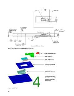
Overview of Optical Mouse Sensor Assembly
Agilent Technologies provides
an IGES file drawing
describing the base plate
molding features for lens and
PCB alignment.
illumination of the surface at
the optimum angle. Features
on the lens align it to the
sensor, base plate, and clip
with the LED.
The components interlock as
they are mounted onto defined
features on the base plate.
The ADNS-2220 clip holds the
LED in relation to the lens.
The LED must be inserted into
the clip and the LED’s leads
formed prior to loading on the
PCB. The clip interlocks the
sensor to the lens, and through
the lens to the alignment
The ADNS-3040 sensor is
designed for mounting on a
through-hole PCB, looking
down. There is an aperture
stop and features on the
package that align to the lens.
features on the base plate.
The HLMP-ED80-PS000 LED is
recommended for illumination.
The ADNS-3120-001 lens
provides optics for the imaging
of the surface as well as
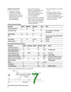
43.13
1.698
42.53
1.674
39.06
1.538
29.50
1.161
1.50
0.059
3.55
0.140
2 X φ
1.00
0.039
28.13
1.107
1.22 3.22
0.048 0.127
15.88
0.625
13.88
0.546
12.60
11.38
0
0.496
0.448
7.60
0.299
1.28
0.050
5.06
0.199
Clear Zone
0
0.80
0.031
Recommended
20X φ
Dimensions in millimeters / inches
Figure 3. Recommended PCB mechanical cutouts and spacing
3

 AGILENT [ AGILENT TECHNOLOGIES, LTD. ]