Ambassador T8100A, T8102, and T8105
H.100/H.110 Interfaces and Time-Slot Interchangers
Advance Data Sheet
November 1999
Table of Contents (continued)
Page Figures
Contents
Page
3.4.2 Setting Up H-Bus Connections....................75
3.4.3 Programming Examples..............................78
3.4.4 Miscellaneous Commands ..........................81
4 Electrical Characteristics ........................................82
4.1 Absolute Maximum Ratings ..............................82
4.2 Handling Precautions........................................82
4.3 Crystal Information............................................83
4.4 Reset Pulse.......................................................83
4.5 Thermal Considerations....................................83
4.5.1 Thermal Considerations for the 208 SQFP.83
4.5.2 Thermal Considerations for the 217 PBGA .83
4.6 dc Electrical Characteristics, H-Bus (ECTF
H.100 Spec., Rev. 1.0)......................................84
4.6.1 Electrical Drive Specifications—CT_C8
and /CT_FRAME............................................84
4.7 dc Electrical Characteristics, All Other Pins......84
4.8 H-Bus Timing (Extract from H.100 Spec.,
Rev. 1.0)............................................................85
4.8.1 Clock Alignment .........................................85
4.8.2 Frame Diagram ...........................................85
4.8.3 Detailed Timing Diagram.............................86
4.8.4 ac Electrical Characteristics, Timing,
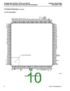
Figure 1. 208 SQFP—Top View................................. 6
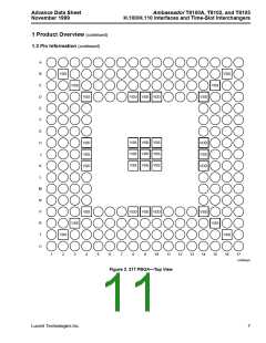
Figure 2. 217 PBGA—Top View................................. 7
Figure 3. Block Diagram of the TSI Devices............. 14
Figure 4. Local Bus Section Function....................... 23
Figure 5. Local Bus Memory Connection Modes...... 24
Figure 6. Local Streams, Memory Structure............. 25
Figure 7. Local Memory (T8100A, T8105 Only),
Fill Patterns ............................................... 26
Figure 8. Simplified Local Memory State
Timing, 65.536 MHz Clock ........................ 29
Figure 9. CAM Architecture ...................................... 31
Figure 10. Simplified H-Bus State Timing,
65.536 MHz Clock................................... 33
Figure 11. Illustration of CAM Cycles ....................... 35
Figure 12. Subrate Switching Example .................... 39
Figure 13. Modifications for Subrate Switching ........ 41
Figure 14. Unpacking Example Using Local
Loopback................................................. 42
Figure 15. Constant Delay/Minimum Delay
Example .................................................. 43
Figure 16. Clocking Section...................................... 44
Figure 17. A, B, and C Clock Fallback State
Diagram................................................... 47
Figure 18. Programming Sequence.......................... 48
Figure 19. Frame Group Output Options.................. 61
Figure 20. External Connection to PLLs................... 71
Figure 21. Physical Connections for H.110 .............. 72
Figure 22. Local-to-Local Connection
Programming (T8100A, T8105 Only) ...... 74
Figure 23. CAM Programming, H-Bus-to-Local
Connection .............................................. 76
Figure 24. Clock Alignment ...................................... 85
Figure 25. Frame Diagram ....................................... 85
Figure 26. Detailed Timing Diagram......................... 86
Figure 27. Detailed Clock Skew Diagram................. 88
Figure 28. ac Electrical Characteristics,
H-Bus (H.100 Spec., Rev. 1.0)....................87
4.8.5 Detailed Clock Skew Diagram.....................88
4.8.6 ac Electrical Characteristics, Skew
Timing, H-Bus (H.100 Spec., Rev. 1.0).......88
4.8.7 Reset and Power On...................................89
4.9 ac Electrical Characteristics, Local Streams,
and Frames.......................................................89
4.10 ac Electrical Characteristics, Microprocessor
Timing .............................................................91
4.10.1 Microprocessor Access Intel Multiplexed
Write and Read Cycles..............................91
4.10.2 Microprocessor Access Motorola Write
and Read Cycles.......................................92
4.10.3 Microprocessor Access Intel Demultiplexed
Write and Read Cycles..............................93
5 Outline Diagrams....................................................94
5.1 208-Pin Square Quad Flat Package (SQFP)....94
5.2 217-Ball Plastic Ball Grid Array (PBGA) ...........95
6 Ordering Information...............................................96
Appendix A. Application of Clock Modes...................97
Appendix B. Minimum Delay and Constant
Local Streams, and Frames .................... 90
Figure 29. Microprocessor Access Intel
Multiplexed Write Cycle........................... 91
Figure 30. Microprocessor Access Intel
Multiplexed Read Cycle........................... 91
Figure 31. Microprocessor Access Motorola
Write Cycle .............................................. 92
Figure 32. Microprocessor Access Motorola
Read Cycle.............................................. 92
Figure 33. Microprocessor Access Intel
Delay Connections..............................103
B.1 Connection Definitions....................................103
B.2 Delay Type Definitions....................................104
B.2.1 Exceptions to Minimum Delay...................105
B.2.2 Lower Stream Rates.................................105
B.2.3 Mixed Minimum/Constant Delay ...............106
Appendix C. CAM Readback and Pattern
Demultiplexed Write Cycle ...................... 93
Figure 34. Microprocessor Access Intel
Demultiplexed Read Cycle ...................... 93
Fill Mode .............................................107
Lucent Technologies Inc.
3

 AGERE [ AGERE SYSTEMS ]