Ambassador T8100A, T8102, and T8105
H.100/H.110 Interfaces and Time-Slot Interchangers
Advance Data Sheet
November 1999
Table of Contents
Contents
Page
Contents
Page
1 Product Overview .....................................................1
1.1 Features..............................................................1
1.2 Description..........................................................1
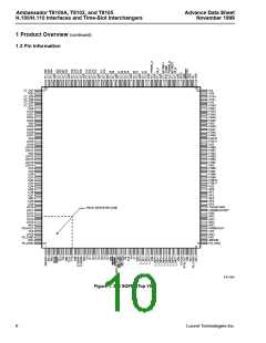
1.3 Pin Information....................................................6
1.4 Ambassador TSI Architecture ...........................12
1.5 Selecting Between T8105, T8102, T8100A,
and T8100.........................................................12
1.6 Enhanced Local Stream Addressing.................12
1.7 Full H.100 Stream Address Support .................12
1.8 Onboard PLLs and Clock Monitors...................12
1.9 Phase Alignment of Referenced and
Generated Frames............................................12
1.10 Interfaces ........................................................13
1.10.1 Microprocessors........................................13
1.10.2 Framing Groups ........................................13
1.10.3 General-Purpose Register and I/O............13
1.11 Applications.....................................................13
1.12 Application Overview ......................................13
2 Architecture and Functional Description.................13
2.1 Register/Memory Maps.....................................15
2.1.1 Main Registers ............................................15
2.1.2 Master Control and Status Register............15
2.1.3 Address Mode Register...............................16
2.1.4 Control Register Memory Space .................17
2.2 Local Bus Section .............................................23
2.2.1 Constant Frame Delay and Minimum
2.5.2 Dividers and Rate Multipliers...................... 45
2.5.3 State Machines........................................... 45
2.5.4 Frame Sync................................................ 45
2.5.5 Bit Sliding (Frame Locking) ........................ 45
2.5.6 MTIE........................................................... 46
2.5.6.1 MTIE Compliance ................................. 46
2.5.6.2 Relationship of the Bit Slider to MTIE ... 46
2.5.6.3 Using the Bit Slider ............................... 46
2.5.7 Clock Fallback............................................ 47
2.5.8 Clock Control Register Definitions.............. 49
2.5.8.1 Basic Fallback Mode............................. 54
2.5.8.2 CKMD, CKND, CKRD: Clocks, Main,
NETREF, Resource Dividers
0x07, 0x08, 0x09 .................................. 55
2.5.9 LREF Pairing.............................................. 57
2.5.9.1 LREF Port Configuration....................... 57
2.5.9.2 Operation.............................................. 58
2.5.9.3 Example of LREF Pairing on a T8100A 58
2.5.9.4 Advantages of LREF Pairing ................ 58
2.6 Interface Section .............................................. 58
2.6.1 Microprocessor Interface............................ 58
2.6.2 General-Purpose Register.......................... 58
2.6.3 Framing Groups ......................................... 59
2.6.3.1 Frame Group Timing............................. 60
2.7 Error Registers................................................. 62
2.8 The JTAG Test Access Port............................. 64
2.8.1 Overview of the JTAG Architecture............ 64
2.8.2 Overview of the JTAG Instructions............. 64
2.8.3 Elements of JTAG Logic............................. 65
2.9 Testing and Diagnostics................................... 66
2.9.1 Testing Operations..................................... 66
2.9.2 Diagnostics................................................. 66
3 Using the TSI Devices........................................... 69
3.1 Resets.............................................................. 69
3.1.1 Hardware Reset ......................................... 69
3.1.2 Software Reset........................................... 69
3.1.3 Power-On Reset......................................... 69
3.2 Device Settings ................................................ 70
3.2.1 Architecture ................................................ 70
3.3 Basic Connections ........................................... 71
3.3.1 LPUE Control Pins ..................................... 71
3.3.2 H.100/H.110 Data Pin Series
Delay Connections......................................24
2.2.2 Serial and Parallel.......................................24
2.2.3 Data Rates and Time-Slot Allocation ..........25
2.2.4 LBS: Local Stream Control, 0x0C ...............28
2.2.5 State Counter Operation .............................29
2.2.6 Software to Reset the Local Connection
Memory .......................................................29
2.3 H-Bus Section...................................................30
2.3.1 Memory Architecture...................................30
2.3.2 CAM Operation and Commands.................32
2.3.3 H-Bus Access..............................................36
2.3.4 L-Bus Access ..............................................37
2.3.5 H-Bus Rate Selection and Connection
Address Format...........................................37
2.4 Subrate Switching for the Ambassador
Family................................................................39
2.4.1 Description, Operation, and Application......39
2.4.2 Definitions ...................................................39
2.4.3 Subrate Switching on H.100/H.110 .............39
2.4.4 Using the Existing Architecture ...................40
2.4.5 Limitations...................................................42
2.4.6 Minimum vs. Constant Delay.......................43
2.4.7 Example of a Practical Application..............43
2.5 Clocking Section ...............................................43
2.5.1 Clock and NETREF Selection .....................45
Termination ................................................ 71
3.3.3 H.110 Hot Swap ......................................... 71
3.3.4 Physical Connections for H.100 ................. 72
3.3.5 Physical Connections for H.110 ................. 72
3.3.6 PC Board BGA Considerations .................. 72
3.4 Using the LAR, AMR, and IDR for
Connections ..................................................... 73
3.4.1 Setting Up Local Connections (T8100A,
T8105 Only)................................................ 73
2
Lucent Technologies Inc.

 AGERE [ AGERE SYSTEMS ]