Ambassador T8100A, T8102, and T8105
H.100/H.110 Interfaces and Time-Slot Interchangers
Advance Data Sheet
November 1999
■ CKR is programmed to 0x50, which sets the PLL
multiplier to 32.
2 Architecture and Functional Descrip-
tion (continued)
■ The resource divider, CKRD, is programmed to 0x03,
which divides the 8.192 MHz clock by 4.
2.5 Clocking Section (continued)
■ The T8100A derives its memory and state machine
clocks from the 8.192 MHz input on LREF0.
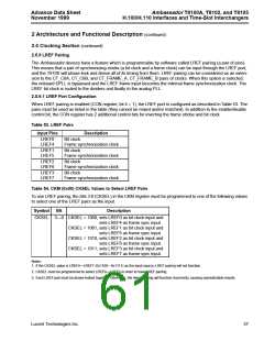
2.5.9 LREF Pairing (continued)
2.5.9.2 Operation
■ The frame synchronization clock will be input to the
state machines, and the T8100A will phase lock to
the framer's 8 kHz clock that is input on LREF4.
If LREF pairing is enabled and CKM has a CKSEL
value of 0x1000 to 0x1011, then the corresponding
internal frame event is sent to the main clock genera-
tion circuit in order for the internally generated clocks to
synchronize to the frame event. The T8100A, T8102,
and T8105 only synchronize to the frame inputs on
LREF[7:4]. The frame input on LREF[7:4] becomes the
internal frame synchronization signal. Also, since the
devices will derive their timing from the bit clock input
on LREF[3:0], the divider(s) and CKR must be pro-
grammed.
2.5.9.4 Advantages of LREF Pairing
LREF pairing provides the user of the T8100A, T8102,
or T8105 with another option for selecting a pair of
clocks from which to derive internal timing. With the
use of the CON register, the user has a very flexible
arrangement regarding the orientation of the LREF pair
that can be input to the T8100A, T8102, or T8105.
The inverting bit in the CON register, bit 2, causes the
bit clock to be inverted. This allows the sampling of the
frame (LREF[7:4]) to occur on either the rising or falling
edge of the bit clock input on LREF[3:0]. The inverting
bit in the CON register, bit 3, causes the frame clock to
be inverted. This allows the internal clock generator to
synchronize to either a rising or falling transition of the
frame input on LREF[7:4].
2.6 Interface Section
2.6.1 Microprocessor Interface
The grouping of the read, write, chip select, and
address latch enable signals, along with the data bus
and the address bus, permit access to the devices
using Intel nonmultiplexed interface (ALE = low), Motor-
ola nonmultiplexed interface (ALE = high), or Intel multi-
plexed interface (ALE = active). ALE controls the
microprocessor mode. All control and status registers
and data and connection memory accesses are con-
trolled through this interface. All accesses are indirect,
following the pin descriptions in Table 1 and Table 2.
Programming examples and a more detailed discus-
sion of the indirect accesses can be found in Section 3
Using the TSI Devices.
The divider registers must be set up for the correct
divide factor. The register that is programmed depends
on which path is chosen. If the LREF bit clock is, for
example, 8.192 MHz and it is not going to be sent to
the PRIREFOUT for external jitter attenuation, then the
resource divider would be programmed. A value of
0x03 gives a divide by 4, and the input to the analog
PLL is 2.048 MHz. The CKR register also has to be
programmed for the correct PLL multiplier. Another fea-
ture of LREF pairing is that the bit clock does not have
to be 8.192 MHz. For example, a 1.544 MHz clock can
be input, sent to PRIREFOUT, and converted to a
2.048 MHz clock, which is then input on the 4MHzIN
pin.
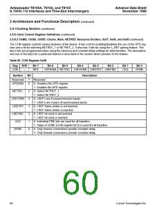
2.6.2 General-Purpose Register
A simple, general-purpose I/O register is available. The
GPR has eight dedicated pins. The GPR corresponds
with I/O pins GP[0:7]. GP6 and GP7 are unavailable if
bit 5 of register CKN is low (see Section 2.5.8 Clock
Control Register Definitions).
2.5.9.3 Example of LREF Pairing on a T8100A
■ The T8100A PCI card has a framer on it and two
phase-locked clock outputs:
— An 8 kHz frame clock going to LREF4.
— An 8.192 MHz bit clock going to LREF0.
The GPD register (0x17) is a write-only register. It sets
the direction bit in the GPR register (0x18). To verify
what is written to the GPD register, the GPR register
has to be read and the direction bits checked. If a bit in
the GPD is zero, the corresponding bit in the GPR is
set to one and the pin is configured as an input. If a bit
in the GPD is a one, then the corresponding bit in the
GPR is zero and the pin is configured as an output.
Also, bit 6 in the CON register (0x0E) must be set to
one to enable writing of the GPD register. Since the
GPD is a write-only register, software will have to keep
track of the current GPR settings, which reflect what is
in the GPD.
■ The CON register is programmed for LREF pairing:
LREFENB bit 4 = 1.
■ The frame strobe and the bit clock are not inverted,
so LREFIFS bit 3 = 0 and LREFIBC bit 2 = 0.
■ The CKM register is programmed to be a master with
phase and snap alignment, and CKSEL[3:0] is set for
LREF0. The value of CKM is, therefore, 0xA8.
58
Lucent Technologies Inc.

 AGERE [ AGERE SYSTEMS ]