Ambassador T8100A, T8102, and T8105
H.100/H.110 Interfaces and Time-Slot Interchangers
Advance Data Sheet
November 1999
2 Architecture and Functional Description (continued)
2.5 Clocking Section (continued)
2.5.9 LREF Pairing
The Ambassador devices have a feature which is programmable by software called LREF pairing (a pair of pins).
This means that a pair of synchronizing clocks (a bit clock and a frame clock) can be input through the LREF port,
and the T810X will phase-lock and derive all of its timing from them. LREF pairing can be considered as an exten-
sion to the CT_C8A, CT_C8B, and CT_FRAME_A, CT_FRAME_B pairs of clocks. When this option is selected,
the onboard DPLL is bypassed and the LREF frame input becomes the internal frame synchronization clock. The
LREF bit clock is routed to the dividers and finally to the analog PLL.
2.5.9.1 LREF Port Configuration
When LREF pairing is enabled (CON register, bit 4 = 1), the LREF port is configured as described in Table 53. The
pairs must be used as listed in the table (they cannot be mixed and/or matched). In addition to the enable/disable
control bit, the CON register has 2 additional control bits for inverting the frame strobe and bit clock.
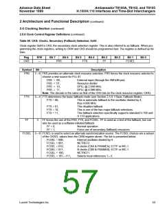
Table 53. LREF Pairs
Input Pins
Description
LREF0
LREF4
Bit clock
Frame synchronization clock
LREF1
LREF5
Bit clock
Frame synchronization clock
LREF2
LREF6
Bit clock
Frame synchronization clock
LREF3
LREF7
Bit clock
Frame synchronization clock
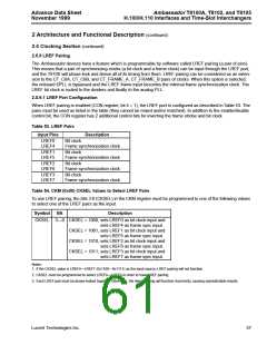
Table 54. CKM (0x00) CKSEL Values to Select LREF Pairs
To use LREF pairing, the bits 3:0 (CKSEL) in the CKM register must be programmed to one of the following values
to select one of the LREF pairs as the input.
Symbol
Bit
Description
CKSEL 3—0 CKSEL = 1000, sets LREF0 as bit clock input and
sets LREF4 as frame sync input.
CKSEL = 1001, sets LREF1 as bit clock input and
sets LREF5 as frame sync input.
CKSEL = 1010, sets LREF2 as bit clock input and
sets LREF6 as frame sync input.
CKSEL = 1011, sets LREF3 as bit clock input and
sets LREF7 as frame sync input.
Notes:
1. If the CKSEL value is LREF4—LREF7 (0x1100—0x1111) as the input source, LREF pairing will not function.
2. CKSEL must be programmed to select LREF0—LREF3 in order to have LREF pairing.
3. Each LREF pair must be phase-locked together. Otherwise, the device timing will function incorrectly, causing unpredictable results.
Lucent Technologies Inc.
57

 AGERE [ AGERE SYSTEMS ]