Ambassador T8100A, T8102, and T8105
H.100/H.110 Interfaces and Time-Slot Interchangers
Advance Data Sheet
November 1999
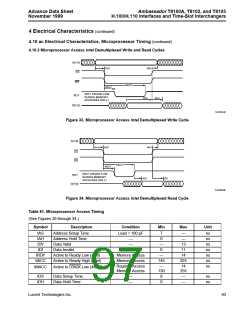
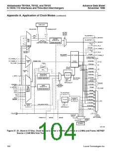
Figure 37 shows an H-MVIP slave arrangement for E1.
In this example, the C16 differential clocks provide the
main source for PLL #1. The 16.384 MHz signal is
divided down to 4.096 MHz and then rate multiplied up
to 65.536 MHz for driving the rest of each device. The
frame sync for the state machines is derived from the
/FRAME and C16 inputs as well as the state informa-
tion provided by C2 and /C4.
Appendix A. Application of Clock
Modes
In the diagrams that follow, four clock modes are illus-
trated using Figure 16, the clocking diagram, as the
basis of each illustration. The key signal paths are
shown in solid lines, and unused paths with narrow
dashes. Two examples also indicate fallback paths. A
register profile (programming values) for all four exam-
ples is on the last page of the appendix.
Note: The bit slider is enabled for a smooth phase
alignment between the internal frame and the
frame sync.
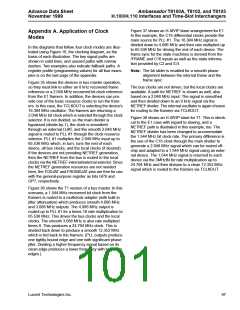
Figure 35 shows the devices in bus master operation,
so they must link to either an 8 kHz recovered frame
reference or a 2.048 MHz recovered bit clock reference
from the E1 framers. In addition, the devices can pro-
vide one of the basic resource clocks to run the fram-
ers. In this case, the TCLKOUT is selecting the device’s
16.384 MHz oscillator. The framers are returning a
2.048 MHz bit clock which is selected through the clock
selector. It is not divided, so the main divider is
bypassed (divide-by-1), the clock is smoothed
through an external DJAT, and the smooth 2.048 MHz
signal is routed to PLL #1 through the clock resource
selector. PLL #1 multiplies the 2.048 MHz input up to
65.536 MHz which, in turn, runs the rest of each
device, all bus clocks, and the local clocks (if desired).
If the devices are not providing NETREF generation,
then the NETREF from the bus is routed to the local
clocks via the NETREF internal/external selector. Since
the NETREF generation resources are not needed
here, the TODJAT and FROMDJAT pins are free for use
with the general-purpose register as bits GP6 and
GP7, respectively.
The bus clocks are not driven, but the local clocks are
available. A path for NETREF is shown as well, also
based on a 2.048 MHz input. The signal is smoothed
and then divided down to an 8 kHz signal via the
NETREF divider. The internal oscillator is again chosen
for routing to the framers via TCLKOUT.
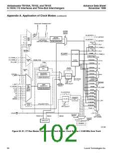
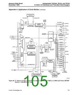
Figure 38 shows an H-MVIP slave for T1. This is identi-
cal to the E1 case with regard to slaving, and a
NETREF path is illustrated in this example, too. The
NETREF divider has been changed to accommodate
the 1.544 MHz bit clock rate. The primary difference is
the use of the C16 clock through the main divider to
generate a 2.048 MHz signal which can be routed off-
chip and adapted to a 1.544 MHz signal using an exter-
nal device. The 1.544 MHz signal is returned to each
device via the 3MHzIN for rate multiplication up to
24.704 MHz and then division to a clean 12.352 MHz
signal which is routed to the framers via TCLKOUT.
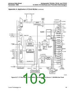
Figure 36 shows the T1 version of a bus master. In this
scenario, a 1.544 MHz recovered bit clock from the
framers is routed to a multiclock adapter (with built-in
jitter attenuation) which produces smooth 4.096 MHz
and 3.088 MHz outputs. The 4.096 MHz output is
routed up to PLL #1 for a times-16 rate multiplication to
65.536 MHz. This drives the bus clocks and the local
clocks. The smooth 3.088 MHz is also rate multiplied
times 8. This produces a 24.704 MHz clock. This is
divided back down to produce a smooth 12.352 MHz
which is fed back to the framers. (PLL outputs produce
one tightly bound edge and one with significant phase
jitter. Dividing a higher-frequency signal based on its
clean edge produces a lower frequency with two clean
edges.)
Lucent Technologies Inc.
97

 AGERE [ AGERE SYSTEMS ]