Data Sheet
March 1997
L7554 Low-Power SLIC
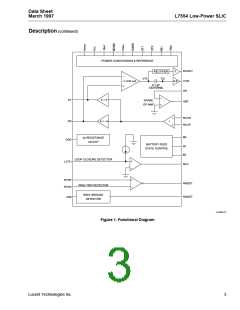
Functional Description
Table 2. Input State Coding
B0 B1 B2
State/Definition
1
1
0
1
1
1
1
0
1
Powerup, Forward Battery. Normal talk and battery feed state. Pin PT is positive with respect to
PR. On-hook transmission is enabled.
Powerup, Reverse Battery. Normal talk and battery feed state. Pin PR is positive with respect to
PT. On-hook transmission is enabled.
Ground Start. Tip drive amplifier is turned off. The device presents a high-impedance (>100 kΩ)
to the PT pin and a current-limited battery to the PR pin. Output pin RGDET indicates current flow-
ing in the ring lead.
0
0
0
1
0
0
0
1
0
Low-Power Scan, Reverse Battery. Except for off-hook supervision, all circuits are shut down to
conserve power. Pin PR is positive with respect to PT. On-hook transmission is disabled.
Low-Power Scan, Forward Battery. Except for off-hook supervision, all circuits are shut down to
conserve power. Pin PT is positive with respect to PR. On-hook transmission is disabled.
Disconnect. The Tip and Ring amplifiers are turned off and the SLIC goes to a high-impedance
state (>100 kΩ).
Table 3. Supervision Coding
Pin NLC
Pin NRDET
Pin RGDET
1 = ring ground
0 = no ring ground
0 = off-hook
1 = on-hook
0 = ring trip
1 = no ring trip
Absolute Maximum Ratings (TA = 25 °C)
Stresses in excess of the absolute maximum ratings can cause permanent damage to the device. These are abso-
lute stress ratings only. Functional operation of the device is not implied at these or any other conditions in excess
of those given in the operational sections of the data sheet. Exposure to absolute maximum ratings for extended
periods can adversely affect device reliability.
Parameter
Symbol
Value
7.0
Unit
V
5 V Power Supply
VCC
Battery (Talking) Supply
VBAT
–75
V
Logic Input Voltage
—
—
–0.5 to +7.0
–7.0 to +7.0
165
V
Analog Input Voltage
V
Maximum Junction Temperature
Storage Temperature Range
Relative Humidity Range
TJ
°C
°C
%
V
Tstg
–40 to +125
5 to 95
RH
Ground Potential Difference (BGND to AGND)
PT or PR Fault Voltage (dc)
PT or PR Fault Voltage (10 x 1000 µs)
Current into Ring Trip Inputs
—
±3
VPT, VPR
VPT, VPR
IRTSP, IRTSN
(VBAT – 5) to +3
(VBAT – 15) to +15
±240
V
V
µA
Note: The IC can be damaged unless all ground connections are applied before, and removed after, all other connections. Furthermore, when
powering the device, the user must guarantee that no external potential creates a voltage on any pin of the device that exceeds the
device ratings. Some of the known examples of conditions that cause such potentials during powerup are the following: 1) an inductor
connected to Tip and Ring can force an overvoltage on VBAT through the protection devices if the VBAT connection chatters, and 2)
inductance in the VBAT lead could resonate with the VBAT filter capacitor to cause a destructive overvoltage.
6
Lucent Technologies Inc.

 AGERE [ AGERE SYSTEMS ]