Data Sheet
March 1997
L7554 Low-Power SLIC
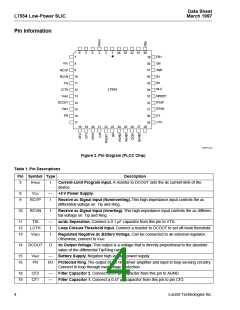
Pin Information (continued)
Table 1. Pin Descriptions (continued)
Pin Symbol Type
Description
20
VITR
O
Transmit ac Output Voltage. This output is a voltage that is directly proportional to the
differential ac Tip/Ring current.
21
ICM
I
Common-Mode Current Sense. To program ring ground sense threshold, connect a
resistor to VCC and connect a capacitor to AGND to filter 50/60 Hz. If unused, the pin can
be left unconnected.
22
RGDET
O
Ring Ground Detect. When high, this open-collector output indicates the presence of a
ring ground. To use, connect a 100 kΩ resistor to VCC.
23
24
25
26
B0
I
State Control Input. B0, B1, and B2 determine the state of the SLIC. See Table 2.
Analog Signal Ground.
AGND
AGND
DCR
—
—
I
Analog Signal Ground.
dc Resistance for Low Loop Currents. Leave open for dc feed resistance of 118 Ω, or
short to DCOUT for 618 Ω. Intermediate values can be set by a simple resistor divider
from DCOUT to ground with the tap at DCR.
27
29
30
BGND
VTX
PT
—
O
Battery Ground. Ground return for the battery supply.
This output is a voltage that is directly proportional to the differential Tip/Ring current.
I/O Protected Tip. The output of the tip driver amplifier and input to loop sensing. Connect to
loop through overvoltage protection.
31
32
RTSN
RTSP
I
I
Ring Trip Sense Negative. Connect this pin to the ringing generator signal through a
high-value resistor.
Ring Trip Sense Positive. Connect this pin to the ring relay and the ringer series resistor
through a high-value resistor.
33 NRDET
O
O
I
Ring Trip Detector Output. When low, this logic output indicates that ringing is tripped.
Loop Detector Output. When low, this logic output indicates an off-hook condition.
State Control Input. B0, B1, and B2 determine the state of the SLIC. See Table 2.
34
35
36
37
38
NLC
B2
B1
I/O State Control Input. B0, B1, and B2 determine the state of the SLIC. See Table 2.
XMT
SN
O
I
Transmit ac Output Voltage. The output of the uncommitted operational amplifier.
Summing Node. The inverting input of the uncommitted operational amplifier. A resistor
or network to XMT sets the gain.
39
40
FB1
FB2
I
I
Forward Battery Slowdown. A 0.1 µF capacitor from FB1 to AGND and from FB2 to
AGND will ramp the polarity reversal transition for added flexibility in applications requiring
quiet polarity reversal. If not needed, the pin can be left open.
Forward Battery Slowdown. A 0.1 µF capacitor from FB2 to AGND and from FB1 to
AGND will ramp the polarity reversal transition for added flexibility in applications requiring
quiet polarity reversal. If not needed, the pin can be left open.
Lucent Technologies Inc.
5

 AGERE [ AGERE SYSTEMS ]