Data Sheet
March 1997
L7554 Low-Power SLIC
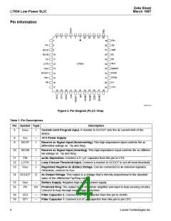
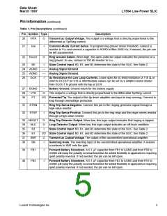
Pin Information
6
5
4
3
2
1
44 43 42 41 40
FB1
SN
7
39
38
37
36
35
V
CC
8
XMT
B1
9
RCVP
RCVN
TXI
10
11
B2
NLC
LCTH
L7554
12
13
34
33
VREG
NRDET
RTSP
DCOUT
14
15
16
17
32
31
30
29
VBAT
RTSN
PR
PT
VTX
18 19 20 21 22 23 24 25 26 27 28
12-2571 (C)
Figure 2. Pin Diagram (PLCC Chip)
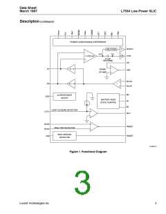
Description
Table 1. Pin Descriptions
Pin Symbol Type
3
IPROG
I
Current-Limit Program Input. A resistor to DCOUT sets the dc current limit of the
device.
8
9
VCC
—
I
+5 V Power Supply.
RCVP
Receive ac Signal Input (Noninverting). This high-impedance input controls the ac
differential voltage on Tip and Ring.
10
RCVN
I
Receive ac Signal Input (Inverting). This high-impedance input controls the ac differen-
tial voltage on Tip and Ring.
11
12
13
TXI
—
ac/dc Separation. Connect a 0.1 µF capacitor from this pin to VTX.
LCTH
VREG
I
I
Loop Closure Threshold Input. Connect a resistor to DCOUT to set off-hook threshold.
Regulated Negative dc Battery Voltage. Can be connected to an external regulator.
Otherwise, connect to VBAT.
14 DCOUT
O
dc Output Voltage. This output is a voltage that is directly proportional to the absolute
value of the differential Tip/Ring current.
15
16
VBAT
—
Battery Supply. Negative high-voltage power supply.
PR
I/O Protected Ring. The output of the ring driver amplifier and input to loop sensing circuitry.
Connect to loop through overvoltage protection.
18
19
CF2
CF1
—
—
Filter Capacitor 2. Connect a 0.1 µF capacitor from this pin to AGND.
Filter Capacitor 1. Connect a 0.47 µF capacitor from this pin to pin CF2.
4
Lucent Technologies Inc.

 AGERE [ AGERE SYSTEMS ]